With the development of carbon materials and their excellent thermal conductivity, more and more research on carbon materials as thermal conductive fillers has become a new research hotspot in academia and industry.

In the thermal interface material industry, carbon materials with higher thermal conductivity are generally used for filling
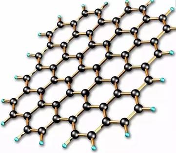
Carbon material is one of the most abundant materials in nature. It has a variety of allotropes. Graphite with layered structure can be formed by sp2 hybridization, and graphene can be stripped from graphite material; Carbon nanotubes can be formed by crimping the network structure of sp2 hybrid arrangement into a ring; While sp3 hybrid can form diamond. In addition, there are amorphous carbon, such as acetylene black, pyrolytic carbon, etc. Because of the differences in the arrangement of carbon atoms, the properties of the structures formed are also very different. For example, diamond is the hardest material found in nature, but graphite can easily fall off due to the weak van der Waals force between layers, and can be used as a pencil lead. Carbon material is a fairly stable material, resistant to chemical corrosion, and in an oxygen-free environment, its high temperature resistance can reach more than 3000 ℃. At the same time, their thermal conductivity is very strong, and they are very promising thermal conductive fillers.
Because the C-C bond in the diamond is very strong, the diamond has high hardness, high melting point and ultra-high thermal conductivity of 2200W/m.k. And all the valence electrons are confined to the covalent bond region without free electrons, so diamond is not conductive and is called "ultimate semiconductor material" by the industry.
Advantages of diamond:
Very high thermal conductivity: thermal conductivity is 2200W/m.K, and diamond has the highest thermal conductivity at room temperature;
Extremely high dielectric breakdown characteristics: the breakdown electric field is 107V/cm, 50 times of GaAs, 2 times of GaN, and 2.5 times of SiC
Extremely high power capacity: the allowable power use capacity is more than 2500 times that of Si material; Especially suitable for making high-power electronic devices;
Low dielectric constant: dielectric constant is 5.7, about 1/2 of GaAs, less than half of InP
High saturated carrier speed: the saturated carrier speed is 12.7 times that of GaAs, Si or InP, and it also maintains high speed when the electric field strength increases;
High carrier mobility: electron mobility is 4500c ㎡/(V · s), higher than most materials, suitable for making high-frequency electronic devices;
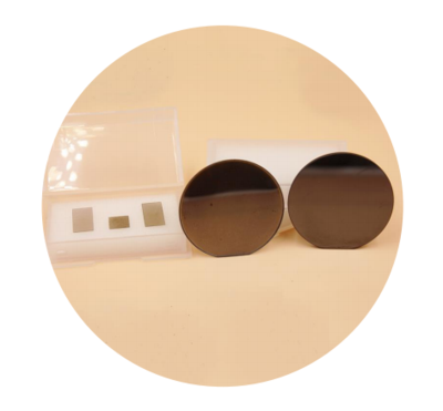
The R&D strength of CVD is at the forefront of the world. The world-class team has accumulated more than 10 years of technology, and has more than 20 international cutting-edge first-class equipment such as MOCVD and PCD. It is the first in China to master the core technology of MPCVD to prepare high-quality diamond and realize mass production. The technical indicators of the core products, diamond heat sink and wafer grade diamond, have reached the world's leading level, and the surface roughness of the wafer grade diamond growth surface Ra<1nm, The thermal conductivity of diamond heat sink is 1000-2000W/m.k.

 闽ICP备2021005558号-1
Leave A Message