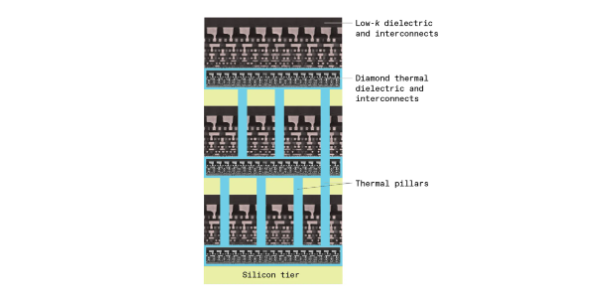
The relentless pursuit of higher performance, greater efficiency, and enhanced thermal management in artificial intelligence (AI) hardware has driven semiconductor research beyond traditional silicon. As AI models grow exponentially in size and complexity, the limitations of conventional silicon-based chips—particularly concerning power density and heat dissipation—have become critical bottlenecks. In this context, diamond wafers are emerging as a transformative material platform with the potential to redefine the future of AI accelerators and high-performance computing.
The Thermal Management Imperative in AI ChipsModern AI chips, such as GPUs and specialized Tensor Processing Units (TPUs), pack billions of transistors into a small area, operating at clock speeds that generate immense heat. This high power density, often exceeding 100 W/cm² in advanced packages, creates a "thermal wall." Excessive heat degrades performance (through thermal throttling), reduces reliability, and increases energy consumption for cooling. Effective heat extraction is no longer just a packaging concern; it is a fundamental determinant of sustained computational throughput. Traditional heat spreaders like copper or even silicon carbide struggle to keep pace with the thermal loads of next-generation AI workloads.

This is where diamond wafers present a paradigm shift. Synthetic diamond, produced via Chemical Vapor Deposition (CVD), possesses exceptional properties:
Extreme Thermal Conductivity: With a thermal conductivity of 2000-2200 W/mK, diamond outperforms copper (~400 W/mK) by a factor of five. It is the best-known thermal conductor at room temperature.
Electrical Insulator: High-quality single-crystal diamond is an excellent electrical insulator, allowing for direct integration without electrical shorting.
Wide Bandgap: Its 5.5 eV bandgap makes it suitable for high-power, high-frequency electronic devices.
Mechanical Strength and Stability: Diamond is extremely hard and chemically inert, offering robustness and reliability.
For AI chips, the primary application of diamond wafers lies in their role as ultra-efficient heat spreaders or as substrates for heterogeneous integration.
Diamond as a Heat Spreader (Passive Cooling)The most immediate application is the integration of a diamond wafer or film as a thermal interface material (TIM) or heat spreader lid directly onto the AI chip's package. By attaching the chip's backside to a diamond wafer, heat generated in the core transistors is rapidly laterally spread across the diamond's surface before being transferred to the heat sink. This drastically reduces "hotspot" temperatures—localized areas of intense heat that can cripple performance. By maintaining a more uniform and lower operating temperature, AI chips can sustain peak clock speeds for longer durations, enabling more consistent training and inference times without triggering throttling mechanisms.
Diamond as a Substrate for Heterogeneous Integration (Active Cooling & More)A more revolutionary approach is to use diamond wafers as the primary substrate for building AI systems. In this heterogeneous integration paradigm, individual compute "chiplets"—specialized for AI tasks like matrix multiplication—are directly bonded onto the diamond wafer. This process, often called direct chip attach (DCA) or using an interposer, places the heat-generating elements in intimate contact with the ultimate heat sink.Furthermore, diamond's properties enable "monolithic" thermal management, where the substrate itself is the cooling solution. Researchers are exploring microfluidic channels etched into the diamond wafer, allowing for direct liquid cooling with unparalleled efficiency. This embedded cooling brings the coolant within micrometers of the transistors, a concept nearly impossible to achieve efficiently with silicon.Beyond thermal management, diamond substrates offer advantages for radio-frequency (RF) components in AI systems. As AI chips integrate more high-speed transceivers for chip-to-chip communication (e.g., in large-scale training clusters), diamond's low dielectric loss and high RF breakdown voltage can improve signal integrity and power efficiency.3. The Future: Diamond for Active DevicesLooking further ahead, the development of electronic-grade single-crystal diamond wafers opens the door to "diamond electronics." Researchers are making progress with diamond-based field-effect transistors (FETs). These devices could operate at voltages and temperatures that would destroy silicon transistors, potentially enabling AI processors to run at higher power densities or in extreme environments (e.g., near-sensor AI in aerospace). While this application is in earlier-stage R&D, it highlights the long-term potential of diamond as an active semiconductor material, not just a passive thermal substrate.
Diamond wafer technology represents a critical innovation vector to overcome the thermal constraints stifling AI hardware progression. By serving as an unmatched thermal conduit, it allows AI chips to operate closer to their theoretical performance limits. Initially as a supreme heat spreader and later as a multifunctional substrate for heterogeneous integration, diamond wafers will enable the design of more compact, powerful, and energy-efficient AI systems. As production scales and costs decline, diamond's role may expand from a thermal management specialist to a foundational platform for the next generation of computing, ensuring that the physical limits of heat do not hinder the exponential growth of artificial intelligence.
CSMH uses the MPCVD method to prepare large-sized and high-quality diamonds,and currently has mature products such as diamond heat sinks, diamond wafers, diamond windows,diamond composite materials,etc.CSMH offers high-quality diamond wafer substrates (e.g., on Si or SiC), whose surface roughness less than 1nm.
 闽ICP备2021005558号-1
Leave A Message