Pos:
Home KnowledgeTechnologyDiamond Heat Sink Wafers: Injecting a "Super Heat Dissipation Engine" into Semiconductor PackagingAs modern semiconductor technology continues to push the limits guided by Moore's Law, an increasingly severe challenge looms large—the thermal management bottleneck. With chip integration soaring to tens of billions of transistors and power density per unit area rising sharply, traditional packaging heat dissipation solutions have become inadequate. In this race against heat, diamond heat sink wafers—hailed as the "ultimate heat dissipation material"—are moving from the lab to the industrial forefront, delivering a revolutionary solution for high-end semiconductor packaging. They are not only critical for unlocking performance but also set to reshape the reliability and future form of high-power-density electronic devices.

Currently, the junction temperature of high-end semiconductor devices—represented by 5G base station RF components, laser diodes, high-performance computing chips, and power modules—directly determines their performance, efficiency, and lifespan. A gallium nitride (GaN) power amplifier operating at full load can see its chip active region temperature instantaneously exceed 200°C. However, traditional heat dissipation substrates based on copper, aluminum, or alumina face a "thermal ceiling" due to their thermal conductivity (copper ~400 W/mK, alumina ~30 W/mK) and thermal expansion coefficient mismatch issues. If heat cannot be dissipated in a timely manner, it will lead to reduced carrier mobility, threshold voltage drift, plummeting efficiency, and ultimately thermal failure. Thus, the primary heat dissipation path inside the package—directly transferring heat from the chip junction to the package shell or heat sink quickly—has become the most critical and challenging link in the entire thermal management chain.
Diamond has the highest known thermal conductivity in nature; the theoretical value of single-crystal diamond at room temperature can reach 2200 W/mK, more than 5 times that of copper. In addition, diamond boasts excellent electrical insulation, a low thermal expansion coefficient (better matched with semiconductor materials such as silicon and GaAs), as well as extreme hardness and chemical stability.
1. Packaging for High-Power RF and Microwave Devices
n 5G/6G communication base stations and phased-array radars, GaN high-electron-mobility transistors (HEMTs) need to output tens or even hundreds of watts of power in the millimeter-wave band. Diamond heat sink wafers play a core role in the packaging of such devices. By directly flip-chip bonding or eutectic bonding GaN chips onto diamond heat sink wafers (i.e., "chip-on-diamond" or "diamond-on-chip" structures), heat generated in the chip active region can be rapidly diffused laterally and conducted downward. Practice has shown that after adopting diamond heat sinks, the junction temperature of GaN devices can be reduced by 40–60°C, output power can be increased by more than 30% at the same temperature rise, and linearity and reliability are significantly improved, providing critical support for a new generation of communication infrastructure.
2. Laser Diode Packaging
High-brightness laser diodes are widely used in industrial processing, medical aesthetics, and lidar. Their luminous efficiency is highly temperature-dependent, and thermal effects cause wavelength drift, reduced output power, and shortened lifespan. By closely mounting the light-emitting region of laser diodes on diamond heat sink wafers, their ultra-high in-plane thermal conductivity rapidly homogenizes and dissipates heat from "hot spots," effectively suppressing thermal-related issues such as "thermal lens effect" and "cat's whisker," and significantly enhancing the brightness, stability, and service life of lasers.
3. Advanced Computing Chip and Power Module Integration
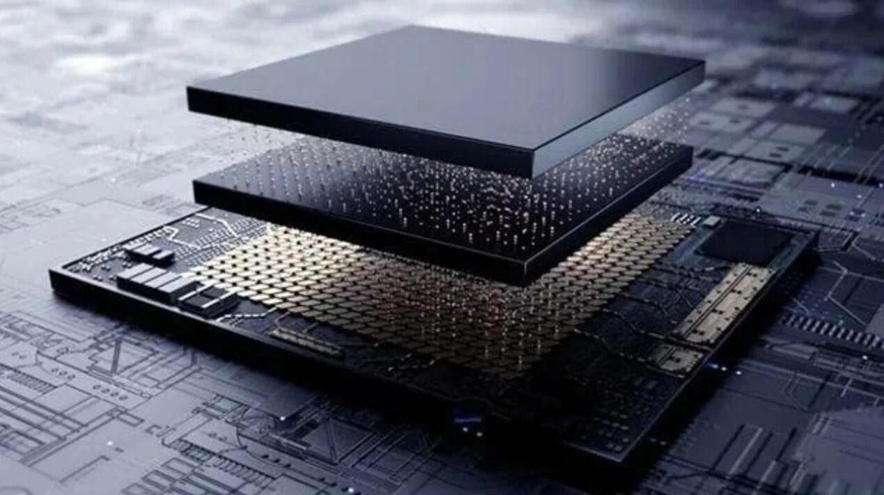
l hot spot issues are particularly prominent in high-performance computing chips such as CPUs and GPUs, as well as IGBT/SiC power modules used in electric vehicles and rail transit. Diamond heat sink wafers can serve as a thermal diffusion layer beneath chips or directly as a substitute for insulated metal substrates (e.g., diamond-copper composite substrates). Inserting a thin diamond wafer between the chip and the package substrate greatly improves the heat transfer path from the chip to the heat sink and reduces thermal resistance. For higher-integration architectures such as 3D stacked chips, interlayer diamond heat sink layers not only conduct heat efficiently but also provide certain mechanical support and electrical isolation, making them a potential key to solving thermal challenges in advanced architectures such as "compute-in-memory."
With their unparalleled thermal conductivity, diamond heat sink wafers are opening up a "superhigh-speed channel" for efficient heat dissipation in the field of high-end semiconductor packaging. They are not only a major upgrade to existing thermal management technologies but also a key enabling technology driving next-generation high-power, high-frequency, and high-integration electronic devices to new heights.
As a leading manufacturer in the diamond semiconductor industry,CSMH uses the MPCVD method to prepare large-sized and high-quality diamonds,and currently has mature products such as diamond heat sinks, diamond wafers, diamond windows,diamond composite materials,etc.Among them,the thermal conductivity of diamond heat sinks is 1000-2200w/(m.k), which has been applied in aerospace, high-power semiconductor lasers, optical communication, chip heat dissipation, nuclear fusion and other fields.
 闽ICP备2021005558号-1
Leave A Message