Pos:
Home KnowledgeTechnologyThe Application of Diamond Wafers in Wafer Bonding for Advanced Semiconductor TechnologiesThe relentless pursuit of higher performance, greater power density, and enhanced thermal management in semiconductor devices has propelled the exploration of novel materials beyond traditional silicon. Among these, diamond emerges as a superlative candidate, boasting exceptional properties such as the highest known thermal conductivity (~2200 W/m·K), high electrical resistivity, wide bandgap (5.5 eV), and outstanding mechanical hardness. The integration of diamond wafers—synthetic, single-crystal or high-quality polycrystalline diamond substrates—into mainstream semiconductor processes represents a frontier in material science. A critical enabling technology for this integration is wafer bonding, which allows the fusion of diamond wafers with other semiconductor materials (e.g., Si, SiC, GaN, Ga₂O₃) to create heterogeneous structures that leverage the strengths of each component.

The primary driver for bonding diamond wafers is thermal management. As transistor densities and operating frequencies increase, power dissipation becomes a bottleneck. Diamond's unparalleled thermal conductivity makes it an ideal "heat spreader" substrate.
High-Power Electronics and RF Devices: Devices based on Gallium Nitride (GaN) or Silicon Carbide (SiC) for radio-frequency (RF) communication and power switching generate immense heat. By directly bonding a GaN-on-Si or GaN-on-SiC wafer to a diamond wafer, the generated heat can be efficiently extracted through the diamond, significantly lowering junction temperatures. This leads to higher operational power, improved reliability, and longer device lifetimes. A notable application is in monolithic microwave integrated circuits (MMICs) for defense and telecommunications.
Wide Bandgap Semiconductor Heterostructures: Diamond itself is an ultra-wide bandgap semiconductor with potential for high-voltage and radiation-hard devices. Bonding single-crystal diamond wafers to other semiconductors (like Ga₂O₃ or AlN) enables the creation of novel heterostructures for sensors, high-temperature electronics, and even quantum information platforms where diamond's nitrogen-vacancy (NV) centers are used.
MEMS and Sensor Packaging: Diamond's mechanical robustness, chemical inertness, and high acoustic velocity make it excellent for micro-electromechanical systems (MEMS) and sensors. Bonding a diamond wafer to a silicon device wafer can provide a hermetically sealed, bio-compatible, and durable capping layer for harsh-environment sensors, resonators, and bio-MEMS.
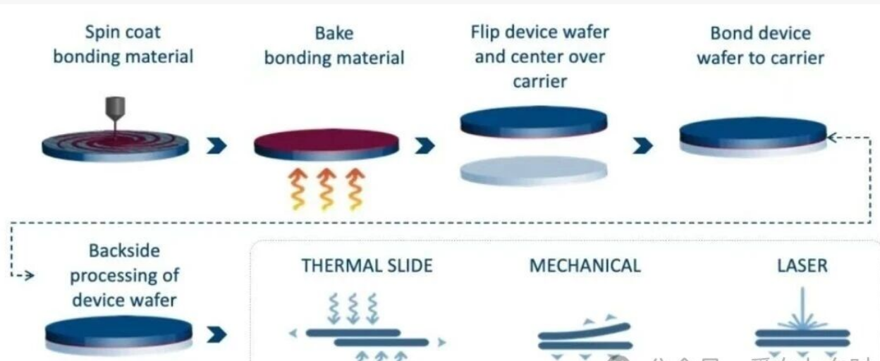
Diamond's chemical inertness and extreme hardness present unique challenges for bonding, precluding conventional fusion bonding used for silicon. Several adapted techniques are employed:
Surface Activated Bonding (SAB): This is a predominant method for diamond bonding. The process involves cleaning and then activating the surfaces of both the diamond and target wafer (e.g., Si, SiO₂, AlN) using an argon fast atom beam or plasma in an ultra-high vacuum chamber. This activation creates dangling bonds and an atomically clean interface. The wafers are then pressed together at room temperature, forming strong covalent bonds. SAB is attractive as it avoids high temperatures that could induce thermal stress due to diamond's low thermal expansion coefficient.
Metal-Based Bonding: This involves depositing intermediate metal layers (e.g., Au, Au-Sn, Ti/Pt/Au) on both wafers. The wafers are then aligned and bonded using thermo-compression. The bonding occurs through the formation of intermetallic compounds or solid-state diffusion at the metal interface. While this can provide excellent thermal and electrical conductivity, it introduces additional materials and potential failure points at the interfaces under thermal cycling.

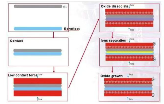
Dielectric Bonding (Anodic or Fusion): For applications requiring electrical insulation, bonding through dielectric layers like SiO₂ is used. Anodic bonding, applying high voltage at moderate temperatures (300-400°C), can bond diamond to glass or silicon with an oxide layer. Modified low-temperature fusion bonding processes, often with plasma activation, are also being developed to create SiO₂|SiO₂ or SiO₂|Diamond interfaces.
In conclusion, wafer bonding is a pivotal technology for unlocking the transformative potential of diamond wafers in semiconductor applications. By enabling direct thermal and mechanical coupling between diamond and active device layers, it paves the way for a new generation of ultra-high-power, high-frequency, and robust electronic systems. While significant material and process challenges persist, ongoing advancements in bonding techniques and diamond synthesis promise to integrate this ultimate material into the heart of future semiconductor technology, pushing the boundaries of performance and efficiency.
CSMH uses the MPCVD method to prepare large-sized and high-quality diamonds,and currently has mature products such as diamond heat sinks, diamond wafers, diamond windows,diamond composite materials,etc.CSMH offers high-quality diamond wafer substrates (e.g., on Si or SiC), whose surface roughness less than 1nm.
 闽ICP备2021005558号-1
Leave A Message