Pos:
Home KnowledgeTechnologyDiamond Wafer: A Revolutionary Thermal Management Solution for Next-Generation Power DevicesDiamond substrates, with their ultra-high thermal conductivity, can significantly enhance the heat dissipation capability of GaN devices and effectively address thermal management challenges under high power density. However, interface bonding stability and thermal resistance control remain key challenges. In the future, they hold broad application prospects in radio frequency (RF), power, microwave, and even ultra-wide bandgap semiconductor devices.
The development of consumer electronics toward high frequency and high power has driven the demand for devices with high output power and efficient heat dissipation. Gallium nitride (GaN), owing to its excellent properties such as high breakdown field strength and high electron mobility, has become the core material for next-generation power electronic devices. GaN high-electron-mobility transistors (HEMTs) are widely used in fields like radar and 5G communications, with a theoretical output power density exceeding 40 W/mm. Nevertheless, the core challenge lies in heat dissipation: the heat generated during high-power continuous operation cannot be effectively dissipated, leading to an increase in junction temperature. As a result, the power density of actual commercial devices only reaches 3–8 W/mm, which severely limits the potential of GaN materials.
Diamond, with its ultra-high thermal conductivity (~2200 W/m·K, 10 times that of silicon), has emerged as an ideal heat dissipation solution, boasting excellent stability and reliability. GaN-on-diamond technology is the primary approach to realizing this solution, which includes three types of manufacturing methods:
Direct bonding of GaN to diamond substrate: The original substrate (e.g., SiC) is stripped off, and after surface activation treatment (e.g., SAB technology), it is bonded to diamond to achieve minimal interface thermal resistance;
Epitaxial growth of GaN on diamond substrate;
Epitaxial growth of diamond on GaN.

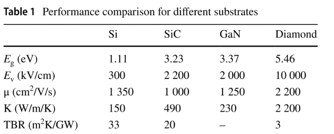
The ultra-high thermal conductivity of diamond stems from the strong sp³ covalent bonds and small mass of carbon atoms in its cubic lattice, forming a rigid structure with high vibration frequency (Debye temperature ~2220 K) that enables efficient phonon heat transfer; the single-crystal structure minimizes grain boundary scattering, resulting in extremely low phonon scattering at application temperatures. Core advantages of GaN-on-diamond: 1. The interface thermal resistance (TBR) can be as low as 3 m²K/GW (significantly lower than that of Si/SiC substrates); 2. Excellent heat dissipation rapidly reduces junction temperature and suppresses gate charge trapping effects (current collapse) under high power; 3. Power density can break through >40 W/mm.
In summary, diamond substrates overcome the bottleneck of self-heating effect (SHE) through ultimate thermal management, serving as a key solution for high-power/high-reliability GaN devices, and are crucial for future structures such as gate-all-around (GAA) FETs and 3D ICs.
Its thermal resistance mainly comes from three parts: (i) the GaN layer itself; (ii) the GaN/substrate interface; (iii) the substrate material. Among them, the thermal resistance of the GaN layer is relatively fixed, and the optimization focus lies in reducing the interface and substrate thermal resistance. Specific strategies include selecting substrates with higher thermal conductivity (e.g., replacing Si/SiC with diamond) or thinning the substrate thickness. Different substrates (Si, SiC, GaN, diamond) exhibit significant differences in thermal conductivity and interface thermal resistance; therefore, special attention must be paid to the thermal resistance management of the GaN-substrate interface to achieve efficient heat dissipation.
Electron-phonon coupling is the core physical mechanism of interface thermal resistance, affecting heat transfer through the interaction between electrons and lattice vibrations: ① Promoting energy transfer from electrons to phonons and increasing the interface lattice temperature; ② Enhancing phonon scattering and reducing the interface thermal conductivity (Figure 5a). In the GaN-on-diamond structure, the strengthened electron-phonon and phonon-phonon coupling significantly reduce the interface thermal resistance (ΔTph-ph decreases in Figure 5b), enabling uniform heat diffusion and effectively suppressing the self-heating effect (SHE). The ultra-high thermal conductivity of diamond combined with optimized interface coupling provides a stable heat dissipation foundation for high-power GaN devices (>40 W/mm).
Numerous experiments have shown that diamond obtained by chemical vapor deposition (CVD) as a substrate can significantly improve the thermal performance of devices under high-frequency and high-power conditions and mitigate SHE. Extensive studies indicate that the utilization of GaN-on-diamond technology offers numerous advantages, including a significant increase in device power, enhanced heat dissipation performance, prolonged device service life, and facilitation of device miniaturization.
There are four traditional diamond-based thermal management methods for heat dissipation: polycrystalline diamond heat dissipation technology (see Figure 8a), single-crystal diamond heat dissipation technology (see Figure 8b), embedded diamond heat dissipation pillar technology (see Figure 8c), and diamond passivation layer technology (see Figure 8d).
GaN devices are widely used in radio frequency and microwave fields due to their high-frequency/high-temperature/high-power advantages, but the self-heating effect (SHE) restricts power density and reliability. Diamond substrates can double the overall thermal performance through near-source efficient heat conduction (theoretical interface thermal resistance as low as 3 m²K/GW), making them a strategic solution to break through the heat dissipation bottleneck.
CSMH uses the MPCVD method to prepare large-sized and high-quality diamonds,and currently has mature products such as diamond heat sinks, diamond wafers, diamond windows,diamond composite materials,etc.CSMH offers high-quality diamond wafer substrates (e.g., on Si or SiC), whose surface roughness less than 1nm.
 闽ICP备2021005558号-1
Leave A Message