Pos:
Home KnowledgeTechnologyGaN Device Diamond Wafer Substrate Growth and Integrated Heat Dissipation TechnologyAs a representative of third-generation semiconductor materials, GaN boasts unique advantages such as excellent electron saturation velocity, breakdown field strength, and band gap. These properties make the comprehensive characteristics of GaN HEMT power devices far superior to those of second-generation semiconductor devices dominated by GaAs. GaN devices are highly suitable for solid-state high-power devices and high-frequency microwave devices, and are widely used in fields such as radar, base stations, and mobile communications.
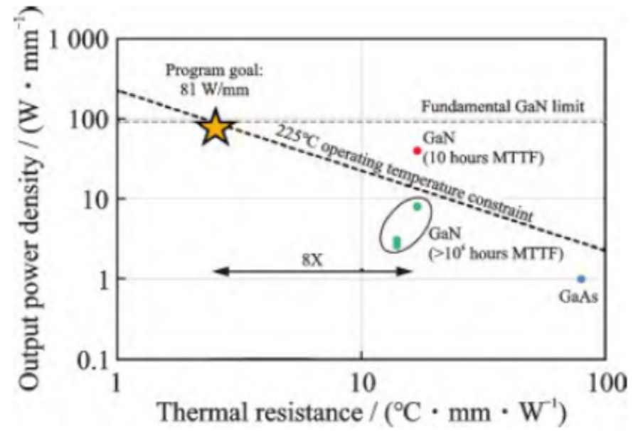
However, with the urgent demand for high-power and high-integration development of new-generation information systems, higher requirements have been put forward for the high power and high power density of GaN devices. The heat accumulation under such high power or high power density leads to a sharp decline in the performance and reliability of GaN devices. Moreover, limited by the heat dissipation structure of GaN devices and the heat transfer capacity of the materials themselves, the high-power potential of GaN devices is far from being realized. Therefore, the heat accumulation problem has become one of the main technical bottlenecks restricting the application and development of GaN devices at this stage.

Utilizing diamond's extremely high thermal conductivity (around 2000 W/mK, 5 times that of copper and 10 times that of aluminum alloy) to dissipate heat in the near-junction region is also a direction to solve the heat dissipation problem of GaN devices. Therefore, the diamond wafer substrate growth and integrated heat dissipation technology for GaN devices is one of the most promising technologies.
The diamond substrate growth and integration technology for GaN devices is led by Raytheon, Element Six, and Qorvo. Its technical scheme is as follows: first, remove the Si or SiC substrate of the GaN epitaxial wafer; then, use microwave plasma technology to grow a diamond substrate on the back of the GaN to realize the self-supporting preparation of the GaN epitaxial wafer with a diamond substrate; finally, fabricate GaN power devices based on the diamond-substrate GaN epitaxial wafer, as shown in the figure below.
The preparation of diamond-substrate GaN epitaxial materials has become the key to this technical approach. Element Six has maturely prepared diamond-substrate GaN epitaxial wafers and collaborated with Qorvo to fabricate diamond-substrate GaN power devices, whose power density is 3.87 times higher than that of traditional GaN power devices. This technical approach requires growing a high-quality diamond substrate on a 1~2 μm GaN epitaxial thin film while ensuring performance indicators such as low stress, low warpage, and large size, which greatly increases the difficulty of the technology. However, its technical advantages are also extremely obvious: the GaN epitaxial wafer with a diamond substrate grown by this technology has lower interface thermal resistance and better thermal resistance uniformity.
A diamond substrate is directly epitaxially grown on the surface of a (111) crystal orientation Si thin film (with a thickness of 410 nm), then a GaN epitaxial functional layer is grown on the other side of the Si thin film to obtain a GaN epitaxial wafer with a Si-diamond composite substrate. Finally, the GaN device tape-out process is carried out to fabricate a diamond-substrate GaN power device with 10 gate fingers and a single gate finger width of 125 μm. Under the same structure comparison, the junction temperature of the diamond-substrate GaN device is 133℃, which is 39℃ lower than that of the traditional SiC-substrate GaN device of the same structure (Qorvo's product, with a junction temperature of 172℃), and the thermal resistance is reduced by 44.8%. When the source-drain voltage is 15 V, the power is increased by 37%.
CSMH uses the MPCVD method to prepare large-sized and high-quality diamonds,and currently has mature products such as diamond heat sinks, diamond wafers, diamond windows,diamond composite materials,etc.CSMH offers high-quality diamond wafer substrates (e.g., on Si or SiC), whose surface roughness less than 1nm.
 闽ICP备2021005558号-1
Leave A Message