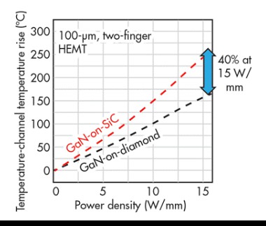
Gallium nitride high electron mobility transistor (HEMT) structures have shown great application in many high power and radio frequency applications due its ability to produce 2-dimensional electron gas (2DEG). Building on silicon electronics technologies, GaN is often grown on Si wafers to allow for efficient manufacture using well established device process and tooling. Current GaN-on-Si devices suffer from poor thermal transport, reducing the effectiveness of the device due to the thermal transport limitations. There is a large drive to utilise the higher thermal conductive materials to help dissipate the excess heat to increase the efficiency of the device. Here we utilise Diamond, which has thermal transport coefficients up to 4 times that of conventional materials, with up to 2000 W/mK. The role of our group in this consortium including the Universities of Bristol, Cardiff, Glasgow and Strathclyde, is to manufacture GaN-on-Diamond and to help characterise Diamond-on-GaN grown by the rest of the consortium.

Fig 1. Channel temperature vs power density for a two finger GaN transistor. GaN on SiC is currently the highest performance technology available. GaN on diamond could deliver at least a 40% reduction in channel temperature for the same power density.
 闽ICP备2021005558号-1
Leave A Message