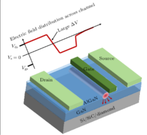
Diamond is five times more thermally conductive (2000) than copper (400), making it ideal for heat dissipation in electronic devices. So if synthetic diamond is used as a chip substrate, the material's thermal conductivity is utilized to more effectively carry heat away from the processor. And since diamond doesn't conduct electricity, the technique is considered a 'best of both worlds' solution, with devices using the material being able to operate in the traditional way while also being more thermally efficient - allowing the chip to run to more power at lower temperatures than currently allowed.
US company Akash buys GPUs from chip suppliers and mounts them on its own diamond GaN PCBs. Their technology reduces the hotspot temperature of GPUs by 10 to 20 degrees Celsius, fan speeds may be reduced by up to 50 percent, overclocking capability increased by 25 percent, and server life may be doubled, saving data centers “millions of dollars in cooling costs” while preventing thermal throttling. In addition, the company says, cooler operation offers RF and satellite system designers a previously unattainable package to increase the communications bandwidth and energy efficiency of satellites while reducing system size, weight and operating costs. In GaN-on-diamond, the heat from the transistors is carried inside the synthetic diamond (the most thermally conductive material ever) substrate, which greatly reduces power amplifier heat generation, resulting in better overall satellite system thermal performance (since, in communications base stations in space, RF power amplifiers are typically responsible for most of the power consumed and heat generated). The cooler operating state of the guard provides RF and satellite system designers with a previously unattainable package to increase the communication bandwidth and energy efficiency of satellites while reducing the size, weight and operating cost of the system.
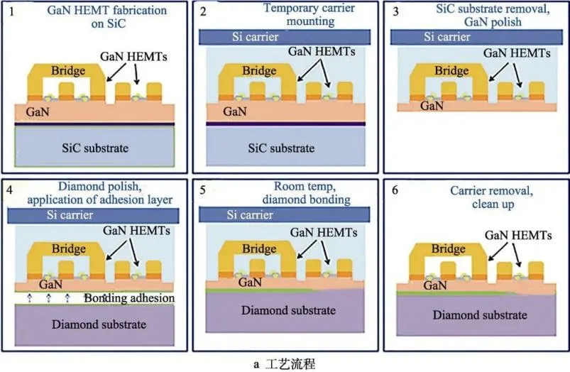
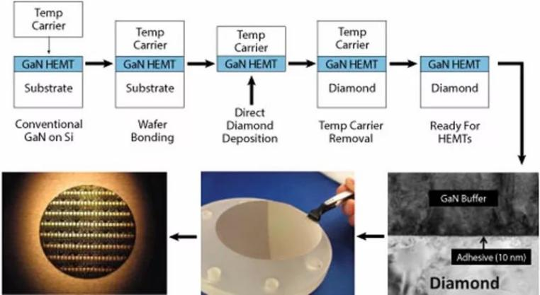
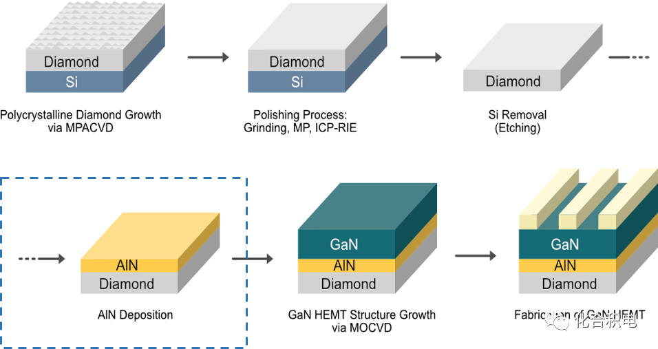
Currently there are three main approaches to preparing diamond substrate GaN-based device technology: based on low temperature bonding technology, based on GaN epitaxial layer growth diamond technology and based on epitaxial growth of gallium nitride on diamond substrates.

1. Low-temperature bonding technique The GaN epitaxial layer is stripped off from the original Si substrate, and then an intermediate layer is added to the exposed GaN surface, which is then bonded to the polycrystalline diamond substrate so that the active region of the GaN-based device is in contact with the CVD diamond substrate and the junction temperature of the power device is lowered.

2. Based on GaN epitaxial layer growth diamond technology with low temperature bonding technology is different from the removal of the substrate and part of the GaN buffer layer in the epitaxial layer on the back side of the first layer of dielectric layer for the protection of the GaN epitaxial layer, and then deposition of diamond substrate (thickness ~ 100 μm). This GaN channel and CVD diamond are close to the most thermally conductive materials in the industry, which greatly reduces the temperature rise between the amplifier substrate and the channel.

3.Epitaxial growth of GaN on diamond substrate In the direct epitaxial growth of GaN structure on diamond substrate, AIN on Diamond, which is developed and produced independently by CSMH, is used as a buffer layer between diamond and GaN, which has the unique and significant advantages of good uniformity, simplification of the epitaxial growth steps, reduction of cost, and reduction of lattice mismatch between the heterogeneous substrate and epitaxial layer, which guarantees the realization of high-quality GaN/AlGaN material epitaxial preparation. It provides a guarantee for the epitaxial preparation of high-quality GaN/AlGaN materials.

CSMH uses the MPCVD method to prepare large-sized and high-quality diamonds, and currently has mature products such as diamond heat sinks, diamond wafers, diamond windows, diamond hetero junction integrated composite substrates, etc. Among them, the thermal conductivity of diamond heat sinks is 1000-2200W/(m.k), and the surface roughness of diamond wafer Ra<1nm. lt has been applied in aerospace, high-power semiconductor lasers, optical communication, chip heat dissipation, nuclear fusion and other fields.
 闽ICP备2021005558号-1
Leave A Message