As the system integration of semiconductor chips develops in the direction of higher density, more functionality, higher power, and intelligence, the heat generation per unit area in the high-performance, high-power processing region within the chip also increases. Usually, the high-performance high-power processing area inside the chip is called the hot spot area. The hot spot area is the main heat source inside the chip, and if the temperature in the hot spot area is high, it will lead to poor overall performance of the chip. Diamond is widely used as a heat dissipation material because of its low dielectric constant, high thermal conductivity, and good mechanical properties.
The application of diamond in semiconductor devices can include package-level diamond soldering, wafer-level diamond bonding, and heterogeneous material diamond coating. Taking heterogeneous material diamond coating as an example, although diamond has high thermal conductivity efficiency, due to the difficulty of forming stable chemical bonds between heterogeneous materials and diamond, the interfacial bonding between diamond heat dissipation layer and heterogeneous materials is poor, and good interfacial bonding can't be realized, which makes the diamond heat dissipation layer easy to fall off. Moreover, during the fabrication process of the diamond heat sink layer, the hydrogen plasma in the nucleation process of the diamond coating may cause etching damage to the surface of the heterogeneous material, resulting in the formation of voids at the interface after the generation of diamond, which also reduces the bonding force of the growth interface. In addition, the grown diamond surface needs to be ground and polished to form the desired diamond heat sink layer, and weak interfacial bonding could easily lead to diamond detachment and failure after grinding and polishing.
Based on this, on December 3, a Chinese well-known technology company announced a patent entitled “a semiconductor device and its production method, integrated circuits, electronic devices”. It is understood that the patent provides a semiconductor device and its production method, integrated circuits, electronic devices, increase the contact area of the diamond heat dissipation layer and the passivation layer, improve the bonding force between the diamond heat dissipation layer and the passivation layer, and improve the thermal efficiency of semiconductor devices by reducing the heat diffusion distance between the diamond heat dissipation layer and the gate.

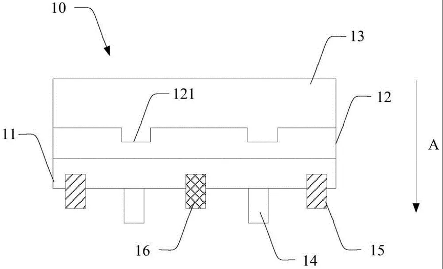
10-semiconductor device, 11-first epitaxial layer, 12-passivation layer, 13-diamond heat sink layer, 14-gate, 15-source, 16-drain, 121-notch The patent shows that the semiconductor device may comprise a first epitaxial layer, a passivation layer and a diamond heat sink layer. Wherein the passivation layer is disposed between the first epitaxial layer and the diamond heat sink layer. A gate is provided on a side of the first epitaxial layer back from the passivation layer. A recess is provided on the surface of the side of the passivation layer facing the diamond heat dissipation layer. Along a thickness direction of the semiconductor device, a projection of the recess on the first epitaxial layer covers at least a portion of the gate. The diamond heat sink layer may cover the passivation layer and fill the recess. In the semiconductor device of the patent, the groove structure of the passivation layer may increase the contact area between the diamond heat sink layer and the passivation layer, thereby increasing the bonding force between the diamond heat sink layer and the passivation layer. As the semiconductor device operates for a longer period of time, the semiconductor device will continuously generate heat, of which more heat is generated in the gate region. The notch can reduce the distance between the gate and the diamond heat dissipation layer along the thickness direction of the semiconductor device, which can reduce the heat diffusion distance between the gate and the diamond heat dissipation layer, and the diamond heat dissipation layer has a larger heat transfer area inside the notch, which can reduce the thermal resistance of the diamond heat dissipation layer, and thus can improve the heat dissipation efficiency of the semiconductor device. In recent years, Huawei has continued to make important progress in the field of diamond heat dissipation. in March 2023, Huawei published two patents on composite thermally conductive materials for chip heat dissipation. The patent specification shows that the two patents use different technical solutions to obtain composite thermally conductive materials for chip heat dissipation, with one technical solution using ferromagnetic particulate material as a thermally conductive filler; the other technical solution uses diamond particulate material as the main heat dissipation material. The two technical solutions have been experimentally verified that the thermal conductivity of the interface thermal conductive materials, such as traditional silicone grease, has been substantially improved. They can be widely used in cell phones, computers, servers and other electronic devices.
These patented technologies fully demonstrate its innovative ability in diamond heat dissipation technology. With the further maturation and application of the technology, it is believed that diamond will play an increasingly important role in the field of semiconductor heat dissipation, providing more efficient solutions to the heat dissipation problems of cell phones, computers and other products.
CSMH uses the MPCVD method to prepare large-sized and high-quality diamonds, and currently has mature products such as diamond heat sinks, diamond wafers, diamond windows, diamond hetero junction integrated composite substrates, etc. Among them, the thermal conductivity of diamond heat sinks is 1000-2200W/(m.k), and the surface roughness of diamond wafer Ra<1nm. lt has been applied in aerospace, high-power semiconductor lasers, optical communication, chip heat dissipation, nuclear fusion and other fields.
 闽ICP备2021005558号-1
Leave A Message