Electronics manufacturing industry as an important support for the development of information technology, has also become an important pillar industry in various countries, China is also in the new period of scientific and technological development program to determine the high-end chips and very large-scale integrated circuits manufacturing industry as a major project. With the development of microelectronics technology, high-density assembly, miniaturization characteristics are more and more obvious, component heat flow density is getting bigger and bigger, the new substrate material requirements are getting higher and higher, requiring higher thermal conductivity, more matching thermal expansion coefficient and better stability. At present, a variety of new encapsulation substrate materials have become the hotspot of the major manufacturers competing for research and development, in which diamond as a new generation of substrate materials are getting more and more attention. At present, the industry will add diamond particles in Ag, Cu, Al and other high thermal conductivity of the metal matrix, the preparation of diamond / metal matrix composite materials, and as a substrate material for electronic packaging, has been initially verified its performance, both with a low coefficient of thermal expansion and high thermal conductivity, has been realized in small-scale applications.
In addition, the era of arithmetic power has sped up as the application of generative AI models such as ChatGPT rages on. Arithmetic power is downwardly rooted in data and upwardly supported by algorithms, which is the core power to drive the development of AI, which has given rise to a new demand for heat dissipation. The heat dissipation of high-performance chips has always been a prominent problem in the service of electronic products, especially in the “post-Moore era”, the power and heat flow density of advanced packaging multi-chip systems have increased dramatically, and the heat flow density of the chip hotspot can even reach the kW/cm2 of the level of the nuclear bomb explosion, which is the limitation of high-performance chip power consumption, arithmetic and integration of the key. This is the key to limit the power consumption, arithmetic and integration of high-performance chips.
For example, Chinese team has developed a low-temperature diamond bonding technology based on reactive nano-metal layers, successfully integrating a polycrystalline diamond substrate into the backside of a 2.5D Interposer package chip, and using a Thermal Test Vehicle (TTV) to study its heat dissipation characteristics.
CSMH uses the MPCVD method to prepare large-sized and high-quality diamonds, and currently has mature products such as diamond heat sinks, diamond wafers, diamond windows, diamond hetero junction integrated composite substrates, etc. Among them, the thermal conductivity of diamond heat sinks is 1000-2200W/(m.k), and the surface roughness of diamond wafer Ra<1nm. lt has been applied in aerospace, high-power semiconductor lasers, optical communication, chip heat dissipation, nuclear fusion and other fields.

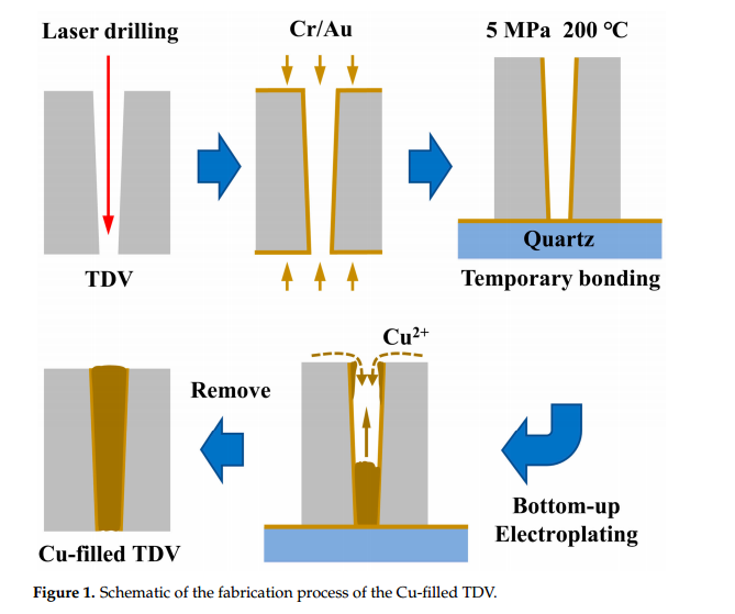
CSMH Diamond TDV Progress

 闽ICP备2021005558号-1
Leave A Message