Pos:
Home KnowledgeTechnologyCVD diamond embedded in chips with significantly reduced IC junction temperatureOver the past two decades, advanced integrated circuits have been evolving in a non-Denardian scale system: circuit sizes are shrinking, single device switching speeds are increasing, but so is the heating power density generated by the circuits. Without mitigation, this leads to higher junction temperatures that limit performance, reliability lifetime, and increase the cost of ownership in data centers due to increased cooling costs. A hallmark of the mitigation approach used over the past two decades is that processor clock speeds stopped growing and computer architectures shifted to multi-core based processors to allow the number of instructions per second to keep growing. This approach and other circuit architectures and operational schemes did not directly address the heat dissipation problem. Consequently, as silicon technology platforms migrated to smaller sized technology nodes, switching times for individual devices became shorter and shorter, while processor speeds remained unchanged. As a result, today's processors are further unable to fully utilize the full performance potential of technology nodes compared to the turn of the century.

Recently, Daniel Lipovitch of Intel, a global leader in the semiconductor industry, in conjunction with Shye Shapira, announced a new advancement on integrating CVD diamond in integrated circuits to reduce device junction temperature. The paper realizes a new approach to meet the growing power density challenge by directly reducing junction thermal resistance by integrating a microcrystalline diamond (MCD) layer in the chip. Processors with integrated MCD layers have the same external dimensions as standard processors, but achieve significantly lower junction temperatures through passive solutions that do not require constant cooling power. One of the more important advantages of increased thermal conductivity is the ability to obtain power performance from a given IC and to emphasize the thermal limiting system. The paper reports the impact of CVD diamond layer integration in chip and advanced Intel processor packages. The integration significantly reduces the junction temperature by 20°C and allows for a performance increase equivalent to advancing a full technology node. The results are published in the journal IEEE under the title “Performance Enhancement of Advanced Integrated Circuits Via CVD Diamond Embedding in a Chip”.

Fig. 1. Thermal impact of the MCD heat sink integrated in the wafer.

Fig. 2. MCD mass production integration scheme.

Fig. 3. Schematic package-level diamond layer integration.

Fig. 4. simulation results.

Fig. 5. Performance Stress Test Benchmark (CB20).

Fig. 6. Example of performance benchmarks for junction temperature reduction through MCD integration compared to standard devices for three high power intensity AI workloads (iSPEC17).

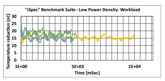
Fig. 7. Example performance benchmarks for various non-computing low-power workloads.
CSMH uses the MPCVD method to prepare large-sized and high-quality diamonds, and currently has mature products such as diamond heat sinks, diamond wafers, diamond windows, diamond hetero junction integrated composite substrates, etc. Among them, the thermal conductivity of diamond heat sinks is 1000-2200W/(m.k), and the surface roughness of diamond wafer Ra<1nm. lt has been applied in aerospace, high-power semiconductor lasers, optical communication, chip heat dissipation, nuclear fusion and other fields.
 闽ICP备2021005558号-1
Leave A Message