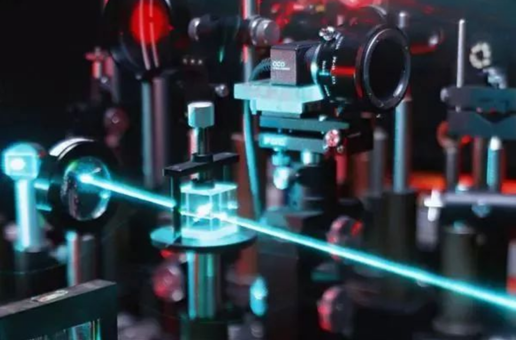
CMSH uses MPCVD equipment to achieve epitaxial growth of polycrystalline diamond material with a thickness of<10um on a 50.8 mm (2 inch) silicon-based gallium nitride HEMT. Scanning electron microscope and X-ray diffractometer were used to characterize the surface morphology, crystalline quality and grain orientation of the diamond film. The results showed that the surface morphology of the sample was relatively uniform, and the diamond grains basically showed (111) plane growth, with Higher crystal plane orientation. In the growth process, the etching of gallium nitride (GaN) by hydrogen plasma is effectively avoided, so that the characteristics of gallium nitride before and after diamond coating do not change significantly.
Submit requirements and contact us
World's First
GaN on Diamond
Grow Diamond on GaN
No Damage to GaN
Customized for Bonding Process
Diamond Wafer(Ra<1nm)
GaN & Diamond
The Best Combination Solution
Combination of GaN & Diamond:
01 Diamond on GaN
Grow diamond on GaN HEMT structures
02 GaN on Diamond
Direct epitaxial growth of GaN structures on diamond substrates
03 GaN/Diamond Bonding
Transfer-bonded to a diamond substrate after GaN HEMT is fabricated
01 Diamond on GaN
CMS uses MPCVD equipment to achieve epitaxial growth of polycrystalline diamond material with a thickness of<10um on a 50.8 mm (2 inch) silicon-based gallium nitride HEMT. Scanning electron microscope and X-ray diffractometer were used to characterize the surface morphology, crystalline quality and grain orientation of the diamond film. The results showed that the surface morphology of the sample was relatively uniform, and the diamond grains basically showed (111) plane growth, with Higher crystal plane orientation. In the growth process, the etching of gallium nitride (GaN) by hydrogen plasma is effectively avoided, so that the characteristics of gallium nitride before and after diamond coating do not change significantly.
02 GaN on Diamond
In the epitaxial growth of GaN on Diamond, CSMH grows aluminum nitride through a special process as GaN epitaxy. The product currently available is Epi-ready-GaN on Diamond (AlN on Diamond).
03 GaN/Diamond Bonding
The technical indicators of CSMH diamond heat sink and wafer-level diamond products have reached the world's leading level. The surface roughness of the wafer-level diamond growth surface is Ra<1nm, and the thermal conductivity of the diamond heat sink is 1000-2000W/m.K. By bonding with GaN, the temperature of the device can also be effectively lowered, and the stability and life of the device can be improved.

application area
MORE 闽ICP备2021005558号-1
Leave A Message