Pos:
Home KnowledgeTechnologySubvert the industry! High-power LED + diamond wafer brings a leap in performance and quality!The key to super-power LED light source technology is its heat dissipation capability. Power densities in the active area of high-power LEDs are extremely high, reaching 1 kW/cm2 or more. Commonly used substrates for traditional high-power LED epitaxial layers are sapphire, silicon carbide and silicon. The thermal conductivity of silicon carbide is about 400 W/(m·K), that of silicon is 140 W/(m·K), that of gallium arsenide is 55 W/(m·K), and that of sapphire is 55 W/(m·K). The thermal conductivity is 25 W/(m·K), even if a silicon carbide substrate is used, it can only be lower than 200 W/cm2. Therefore, the biggest technical bottleneck of ultra-high-power LED devices is heat dissipation. Diamond has the highest thermal conductivity among the materials, reaching 2000 W/(m·K). It is an ideal substrate material, which can reduce the thermal resistance of the device and improve the power density. Therefore, the manufacture of high-power LEDs with diamond as a substrate has become a research hotspot.
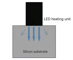
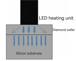
The researchers deposited a diamond thin film heat dissipation layer on the surface of the Si substrate to improve the heat dissipation capability of the LED. For the structure without the diamond film heat dissipation layer (as shown in the figure below, the arrow in the figure is a schematic diagram of the direction and size of the heat flow), the heat dissipation of the LED is to transfer the heat generated at the pn junction to the medium with poor heat dissipation capacity, such as package thermal conductivity. Rubber and silicon substrates have poor thermal conductivity in the horizontal direction, and the heat is concentrated in the place where the LED is in contact with the medium, which belongs to "spot heat dissipation"; after adding a diamond film as a heat dissipation layer, the high thermal conductivity of the diamond film can be used. The high-density heat flow of the point heat source quickly diffuses through the entire diamond film (horizontal and vertical directions), thereby reducing the heat flow density into the Si substrate, greatly improving the heat dissipation capacity, and reducing the junction temperature of the LED.


Schematic diagram of the effect of "point heat dissipation" without diamond heat dissipation layer and "surface heat dissipation" with diamond heat dissipation layer
The application demand of ultra-high-power LED light sources is increasing year by year, and diamond materials with high thermal conductivity play a key role in improving the power density of LEDs, and have broad application prospects. Compared with the most advanced silicon carbide substrate GaN devices, the diamond substrate has a higher surface power density, and the temperature can be reduced by 40% to 45%. The LED light source using the diamond heat dissipation structure not only improves the power, reliability and life of the LED light source by an order of magnitude, but also has a smaller volume and quality compared with the traditional high-power LED light source. Manufacturing costs are also significantly reduced.
CSMH focuses on the R&D and production of diamond wafers. It has excellent R&D capabilities, excellent independent innovation capabilities, more than ten years of technology accumulation, and continuous breakthroughs in core key technologies. It is committed to becoming the world's leading wide-bandgap semiconductor materials and devices. The company's core products are wafer-level diamond heat sinks, GaN-on-diamond epitaxial wafers, aluminum nitride films and piezoelectric materials.
The company has the ability to design MPCVD equipment. It is the first company in China to master the core process of MPCVD to prepare high-quality diamond and realize mass production. It also creates an efficient and precise machining method for the atomic-level surface of diamond based on plasma-assisted polishing. The roughness is reduced from tens of microns to less than 1 nm, reaching the standard of semiconductor-level applications. High-power semiconductor lasers using diamond wafers have been used in optical communications, and are also used in laser diodes, power transistors, and electronic packaging materials.
 闽ICP备2021005558号-1
Leave A Message