Pos:
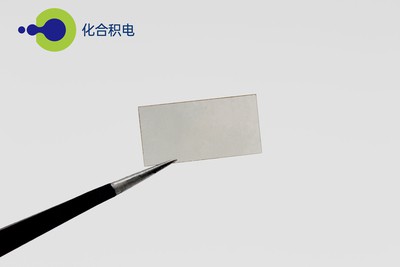
Home KnowledgeTechnologyDiamond heat sink high power semiconductor laser used in optical communicationHigh power semiconductor lasers using diamond heat sink (heat sink) have been used in optical communication. The natural type ⅱ A diamond thermal sink is used to solve the heat dissipation problem of microwave and laser diode devices. The size of diamond thermal sink is about 1mm2, which can only be used for a single laser diode device. The appearance of large area high thermal conductivity CVD diamond film makes it possible for its thermal management applications in high power laser diode array (LDA) and other microelectronics and optoelectronic devices. A typical laser diode array is a laser diode device with an amplitude of 10mm distributed from 200m wide to 600m long at intersections of 200m apart. Diamond film with a length of 10mm is required to be used as thermal conductive sheet, which is no problem for CVD diamond film technology. In the preparation of high thermal conductivity diamond film, the highest thermal conductivity level has reached 18.5 W/M.K, which is capable of preparing large area high thermal conductivity diamond thermal precipitation wafer. Another more attractive application prospect of diamond thermal precipitation is in the ongoing development of McM-multi Chip Modules, which aims to combine many vlSI chips tightly in a three-dimensional manner into ultra-small ultra-high performance devices. The heat dissipation of these chips is the key to this technology, and obviously diamond film is the most ideal material to solve this technical problem.
The advantages of diamond film as a packaging material for microelectronic devices are obvious, because of the high thermal conductivity, high resistivity and good matching with silicon device materials in thermal expansion coefficient. Any existing packaging materials can not be compared with diamond film packaging materials.
Focusing on the research and development and production of diamond,CSMH has made major breakthroughs and progress in the field of diamond heat sink, realizing the technical indexes of diamond thermal sink and wafer level diamond products to reach the world's leading level. The surface roughness of wafer diamond growth surface Ra < 1nm, and the thermal conductivity of diamond heat sink reaches 1000-2000W/m.K.

 闽ICP备2021005558号-1
Leave A Message