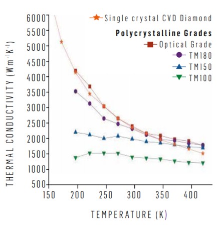
As the third-generation semiconductor material, the thermal conduction and thermal expansion of diamond are particularly concerned. We has been focusing on the research and production of diamonds, providing high-quality diamond heat sink, wafer-level diamonds, diamond coating (GaN) and other products and services under the premise of maintaining the thermal conductivity of diamonds.
Unlike metals, heat conduction in diamond is dominated by lattice vibrations (phonons). The thermal conductivity is then determined by how these are scattered. In diamond, at room temperature, this is related to phononphonon scattering (Umklapp processes) and defect/impurity scattering. With grain size above ~ 50 µm and high phase purity, polycrystalline CVD diamond has been found to have a through plane conductivity varying by less than 10% of its in-plane value.

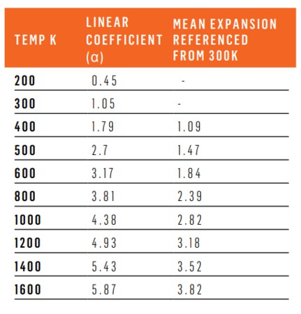
Diamond has an extremely low coefficient of thermal expansion, attributed to the very high bond energy. In general the expansion of materials is related to the phonon characteristics as a function of temperature and generally varies with temperature. Diamond has a low coefficient of thermal expansion at room temperature, rising steadily with temperature, as shown in the table below.

Diamond is a wide bandgap semiconductor, with an indirect gap of 5.47 eV. Experiments on high purity CVD diamond have reported high mobility values and long lifetimes for electrons and holes. Combined with the high breakdown field and thermal conductivity, this makes diamond the preferred material for a number of demanding electronic applications.
Diamond’s radiation hardness arises from its high atomic displacement energy (42eV/atom) and low atomic number. Thus it can demonstrate stable high sensitivity to radiation in comparison to other solid state detector materials.
All known dopants for diamond are deep, however with B > 1 × 10²⁰ atoms cm-3, the acceptor levels overlap with the valence band as the diamond undergoes the Mott transition to demonstrate metal-like p-type conductivity. Due to the activation energy, n-type doping in diamond has only been considered for high temperature and UV applications, with limited success.
Conducting, polycrystalline boron doped diamond (BDD) has the widest solvent window of all electrode materials in aqueous solution. It also has very low background and capacitive currents, and reduced fouling, compared to other electrodes along with the ability to withstand extreme potentials and harsh environments. However these properties are highly dependent on the diamond quality, with the properties improving as the non-diamond-carbon (NDC) content decreases. Free-standing, solid BDD electrodes can be grown with both trace and negligible NDC content.
The very wide solvent window of diamond in aqueous solution pushes out gas evolution to very high cathodic/anodic potentials and enables the generation of highly oxidizing hydroxyl radical, with very high current efficiency. This process can be used in advanced oxidation processes. The inert characteristics of the BDD electrode make it an ideal platform for electrochemical sensing applications.
 闽ICP备2021005558号-1
Leave A Message