The Key Laboratory of Microscopic Magnetic Resonance of USTC has made important progress in the direction of diamond quantum device preparation, developing a new self-alignment-based processing technique for photonics device preparation, which can process the nitrogen-vacancy color center, an atomic-level quantum sensor, to the best working position of the diamond device with nanoscale precision, realizing a quantum sensor array with near-optimal optical detection performance. The research results are published in Science Advances.
Diamond has excellent physical and chemical properties such as high hardness, high stability, high light transmission, high thermal conductivity and ultra-high wide bandgap, and has a wide range of applications in industrial fields such as ultra-precision machining, optical materials and semiconductor electronic devices. In the past decade or so, scientists have discovered that nitrogen-vacancy (NV) color centers, an atomic-scale lattice defect in diamond that can emit light, have great promise for quantum applications, making the imperfect diamond more "perfect" in terms of practicality. "NV color centers can not only measure electromagnetic fields, pressure and other physical quantities with nanometer spatial resolution in room temperature and atmosphere, but also establish multi-body quantum entanglement, which can be used to study quantum information and other fundamental problems, and has significant applications in frontier basic science and high-tech industries.

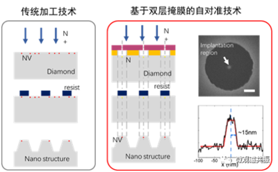
Diagram of Preparation Technology Method
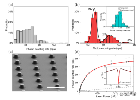
The preparation of high-performance diamond quantum devices is a key technology for the practicalization of diamond quantum information technology. Taking diamond quantum sensors as an example, the principle is to use the NV color center inside the device to convert the weak physical signals from the outside world into its own fluorescence intensity signal for detection, so increasing the NV color center photon counting rate is a key indicator to enhance the sensor performance without sacrificing other physical properties. In the past few years, active efforts have been devoted to the development of diamond micro- and nanophotonic structures for enhancing the fluorescence intensity of NV color centers, such as solid immersion lenses, columnar waveguides, circular bull's-eye gratings, parabolic reflectors, and inverted nanocones. However, the current conventional preparation techniques cannot precisely control the NV color center position in the micro- and nanostructures, resulting in low device preparation efficiency and difficult performance (Figure 2(a)), which is mainly due to the alignment problem between the NV color center preparation process and the diamond structure etching process (Figure 1, left). Usually this alignment accuracy needs to be better than 20 nm to achieve the theoretically optimal optical performance of the optical device.

(a) Optical count rate distribution of devices fabricated by conventional process; (b) Optical count rate distribution of devices fabricated by self-alignment process; (c) Electron micrograph of diamond nanopillar sensing array; (d) Fluorescence saturation curve test of a single NV color center.
For the above problem, the research team in this work developed a photonics device processing technique based on a self-alignment strategy to achieve self-alignment of the nitrogen ion injection process and diamond structure etching process required for generating NV color centers through a double-layer mask patterning process design, which can reach an accuracy of 15 nm (Figure 1, right). Using this technique, the research team achieved the fabrication of a high-performance diamond nanopillar sensing array, which can be used for cutting-edge applications such as biosensing and imaging of nanoscale magnetic materials. The devices show highly consistent and optimal photon counting rates and device yields close to theoretical expectations compared to conventional fabrication techniques. By further controlling the fluorescence emission dipole orientation through diamond crystal orientation, the team finally achieved a saturated photon counting rate of ~4.34 Mcps for a single NV color center and an approximately 20-fold increase in fluorescence intensity (Figure 2). The method is simple and highly accurate, and can be applied to other solid-state quantum systems such as silicon carbide and rare-earth ions, as well as to bulk production of high-performance diamond quantum sensors.
We are the first one in China to master the core process of MPCVD to produce high quality diamond and realize the mass production, and we are the first one to create a plasma-assisted polishing-based diamond atomic-level surface high-efficiency precision processing method, wafer-level diamond Ra<1nm, and diamond thermal conductivity 1000-2000W/m.k. We have GaN on diamond, Diamond on GaN, diamond-based aluminum nitride and other products, which are used to solve the heat dissipation problems of power electronic devices and RF devices in the fields of high frequency, high pressure and high temperature, etc. In the future, we will continue to improve the quality of our products through manufacturing intelligence, optimizing the production process and other measures, benchmarking with the international advanced management level, and continuously improving our products and services.
 闽ICP备2021005558号-1
Leave A Message