Pos:
Home KnowledgeTechnologyFrom Advanced Packaging Thermal Management Challenges to the Industrial Value of Diamond on Si TechnologyThe rapid growth of AI computing power is driving semiconductor architectures to evolve from traditional 2D integration toward 2.5D and 3D advanced packaging. As the integration density of GPUs, HBM, and high-performance computing chips continues to increase, internal heat flux density is rising significantly. Thermal management has become one of the key challenges limiting the development of next-generation computing systems.
In 3D stacking architectures, multiple logic dies and memory dies are vertically integrated. While this approach significantly shortens signal transmission distances and improves system performance, it also introduces new thermal challenges—the generated heat is confined within increasingly smaller spaces, resulting in localized hotspots and thermal accumulation.
Traditional silicon-based materials and copper-based thermal dissipation pathways are gradually approaching their performance limits. Silicon has a thermal conductivity of approximately 150 W/(m·K), while copper reaches around 400 W/(m·K). In contrast, diamond offers an exceptional thermal conductivity exceeding 2,000 W/(m·K), providing outstanding heat spreading capability. As a result, diamond is widely regarded as one of the most promising materials for future high-power semiconductor thermal management.
However, the integration of diamond into the semiconductor industry is far more complex than simply attaching a piece of diamond onto a chip surface.
The key challenge lies in enabling diamond to achieve compatibility with mature silicon-based semiconductor manufacturing ecosystems, which is essential for large-scale industrial adoption.
Conventional diamond thermal management solutions face multiple engineering challenges. The mismatch in coefficients of thermal expansion between diamond and silicon can generate significant interfacial stress. Meanwhile, diamond’s extreme hardness makes wafer processing, polishing, and microstructure fabrication highly challenging. In addition, directly introducing diamond into semiconductor manufacturing processes requires strict compliance with semiconductor-grade requirements for cleanliness, surface uniformity, and long-term reliability.
To address these industry challenges, CSMH has developed an innovative Diamond on Si technology platform. Leveraging its proprietary MPCVD equipment and advanced epitaxial growth processes, CSMH enables direct growth of high-quality diamond films on single-crystal silicon substrates, achieving the integration of ultra-high thermal conductivity diamond materials with established silicon-based semiconductor manufacturing systems.
The core advantage of CSMH’s Diamond on Si technology lies in utilizing silicon as a process-compatible bridge and diamond as a highly efficient thermal transport layer. By optimizing key parameters such as diamond film thickness uniformity and interfacial thermal resistance during the growth process, Diamond on Si maintains compatibility with silicon-based manufacturing processes while introducing diamond’s superior heat spreading capability, providing a more efficient thermal management pathway for advanced packaging applications.
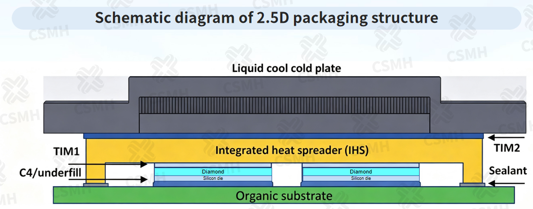
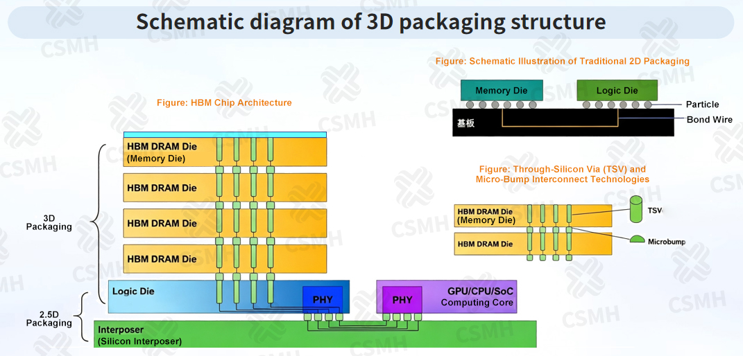
In 2.5D/3D advanced packaging, Diamond on Si can serve as a critical component in high-performance thermal substrates, heat spreading layers, and backside thermal dissipation structures. It enables rapid spreading of localized heat generated by GPUs, CPUs, and AI accelerator chips, reducing hotspot temperatures and improving the operational stability of high-power semiconductor devices.
For future high-density 2.5D/3D stacked architectures, Diamond on Si provides a solution aligned with the direction of semiconductor industry development—preserving the mature advantages of the silicon-based semiconductor ecosystem while overcoming the thermal performance limitations of conventional materials under extreme heat flux conditions.
CSMH remains committed to advancing diamond material innovation and industrialization. Through continuous development of CVD diamond growth technologies and Diamond Heat Sink composite solutions, CSMH is delivering next-generation high-performance thermal management solutions for AI computing chips and advanced semiconductor packaging.
 闽ICP备2021005558号-1
Leave A Message