Pos:
Home KnowledgeTechnologyCSMH Tackles Thermal Coupling Challenges in Advanced Packaging, Enabling Next-Generation Thermal Management for AIAs AI computing continues to advance at a rapid pace, 2.5D and 3D advanced packaging have become mainstream architectures for high-performance chips. With the power consumption of next-generation GPUs continuing to rise, multi-layer chip stacking is creating increasingly severe thermal coupling effects, while localized hotspots are becoming a critical challenge. Conventional copper- and aluminum-based thermal management materials are approaching their physical performance limits, making thermal management a key bottleneck for the large-scale commercialization of high-performance GPUs and CPUs.

Diamond, with an ultra-high thermal conductivity of approximately 2,000–2,200 W/(m·K), combined with a coefficient of thermal expansion (CTE) close to that of silicon and excellent electrical insulation properties, is regarded as a key material for next-generation thermal management in high-end semiconductor applications. However, large-scale commercialization has long been constrained by three major challenges: the difficulty of fabricating large-area diamond films, the low bonding yield associated with diamond–silicon heterogeneous integration, and the high cost of system integration. As a result, diamond-based thermal management solutions have largely remained limited to small-volume applications in aerospace and defense, with limited suitability for the rapidly expanding AI computing and data center markets.
CSMH has developed a fully proprietary Diamond on Si composite heat-spreader solution, establishing a practical bridge between advanced diamond materials and existing silicon-based semiconductor manufacturing processes. The solution provides a scalable thermal management approach for high-power AI chips and advanced packaging. The technology has completed packaging and testing validation for GPU/CPU applications with overseas partners, with mass production scheduled to begin in the second half of 2026.
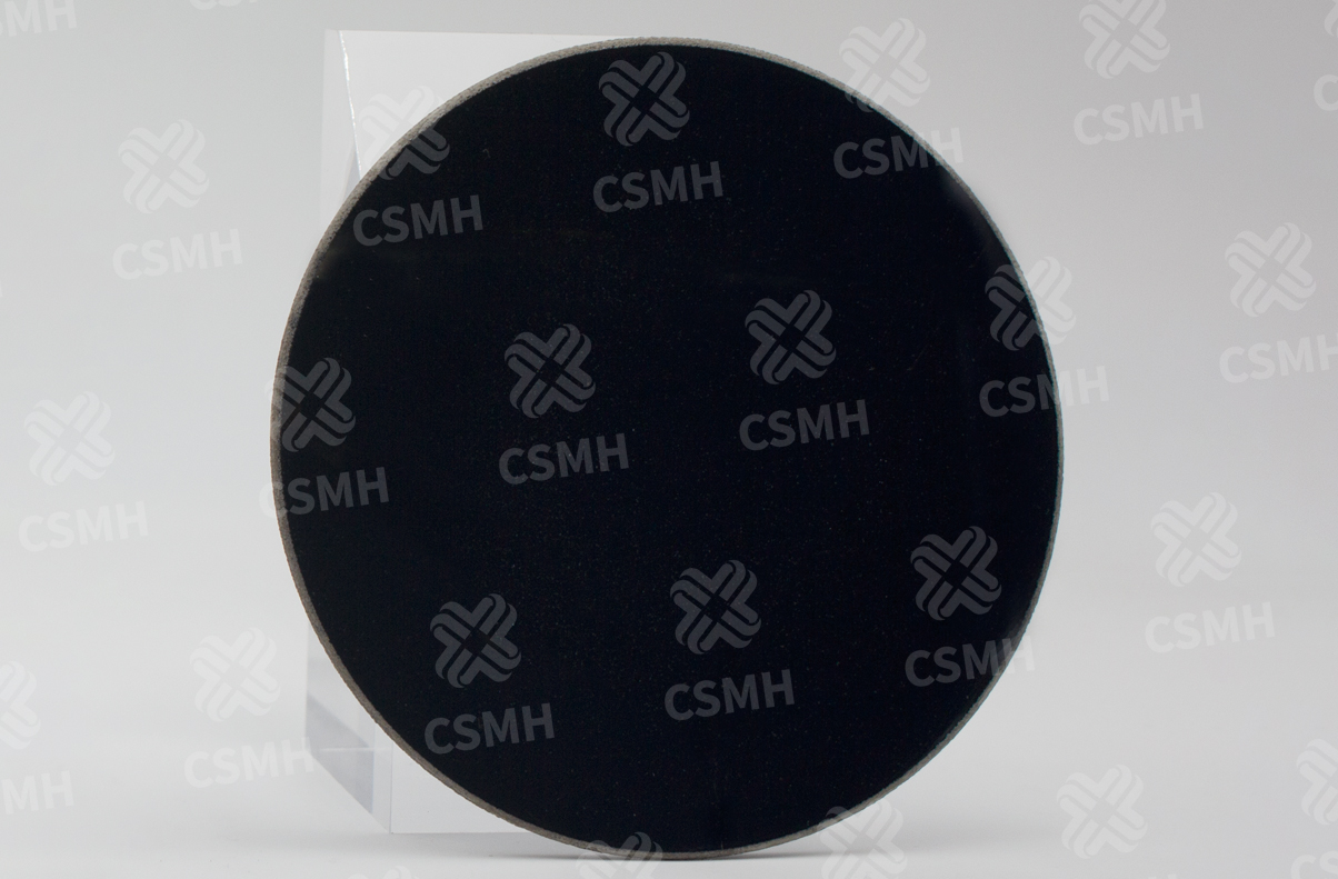
Leveraging its proprietary MPCVD technology, CSMH directly grows polycrystalline diamond films on single-crystal silicon substrates. The silicon substrate is subsequently thinned to form Diamond on Si composite wafers. Through proprietary interface engineering and customized seeding materials, CSMH enables controlled film-thickness uniformity and tunable interfacial thermal resistance, establishing a reproducible process window suitable for industrial-scale manufacturing.
The core innovation lies in transforming the technically challenging and yield-sensitive diamond–silicon heterogeneous bonding process into the mature silicon–silicon homogeneous bonding process widely used in the semiconductor industry. A Diamond on Si wafer is first fabricated and then bonded to the silicon-based epitaxial wafer of the chip. This approach minimizes the need for downstream manufacturers to make extensive modifications to their existing production lines, thereby reducing technology introduction costs and shortening the implementation cycle.
For 2.5D and 3D stacked packaging, the composite substrate can be customized in terms of dimensions and thickness. Its thermal expansion characteristics are well matched with silicon-based chips, helping mitigate thermal coupling effects and reduce the risk of interfacial delamination and failure during high- and low-temperature cycling. Thermal simulations indicate that the solution can reduce the peak junction temperature of a chip by approximately 24°C, significantly suppressing hotspot temperature rise. As a general industry rule of thumb, reducing junction temperature by approximately 10–15°C can potentially reduce device failure rates by around half. Stable temperature reduction can also help minimize thermal throttling and extend device operating lifetime.
In terms of intellectual property, CSMH has established a patent portfolio in key markets including China and the United States, covering the entire technology chain from material fabrication and substrate processing to device integration. The company has also established a digitalized manufacturing facility integrating customized equipment development, precision grinding and polishing, and laser micro/nano cutting, enabling end-to-end in-house development and manufacturing. Its product portfolio includes Diamond-Copper Composite Materials, Diamond Heat Sink, Diamond Flexible Film, and GaN on Diamond, covering a broad range of applications from system-level thermal management and near-chip cooling to embedded thermal management for advanced packaging.
CSMH has developed three differentiated diamond-based thermal management pathways. Diamond-Copper Composite Materials target system-level thermal management for high-power modules; Diamond Heat Sink solutions focus on near-chip thermal management; and CSMH's Diamond on Si substrate is specifically positioned for embedded thermal integration in advanced packaging. Its key competitive advantage lies in its compatibility with existing semiconductor manufacturing processes.
As 2026 marks the beginning of a new phase of industrial-scale adoption of diamond-based thermal management, demand for advanced packaging thermal solutions is expected to accelerate significantly. CSMH will continue to advance process optimization and cost reduction while working closely with upstream and downstream industry partners to accelerate the large-scale adoption of diamond-based thermal management in high-performance computing servers, enabling data centers to achieve higher computing density, improved thermal efficiency, and greater operational reliability.
 闽ICP备2021005558号-1
Leave A Message