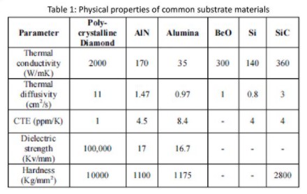
Cutting edge AlGaN/GaN high electron mobility transistors (HEMTs) have achieved RF power densities reaching 40 W/mm. HEMT’s in production are typically limited to around 5-7 W/mm.Current technology typically uses SiC substrates due to its relatively high thermal conductivity (~400 W/m-K)Majority of junction to case resistance comes from ceramic insulating layersDefects at the interface of GaN and SiC lessen thermal performance

Use of diamond can mitigate the near junction thermal resistance (limiting factor for GaN on SiC)Dielectric strength Hardness

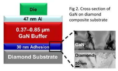
Diamond grown through chemical vapor deposition (CVD) processPoor fabrication techniques will result in defects and increased thermal resistancePrimary method involves transferring pre-grown AlGaN/GaN structures to polycrystalline CVD diamond(diamond heat sink)

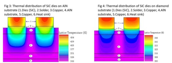
For the same level of power dissipation, GaN-on-diamond HEMT shows over 25% lower temperature rise than GaN-on-SiC

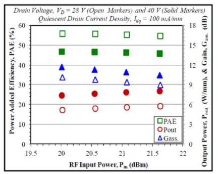
GaN-on-diamond HEMTs recorded a record of over 7 W/mm output power with a 40 V bias at 10 GHz.Good power added efficiency (PAE) (~55%, comparable to GaN-on-SiC)Low level of current collapse (13%, comparable to GaN-on- SiC)

Large mismatch of crystalline properties (lattice constants, coefficients of thermal expansion) make fabrication of high quality GaN-on-diamond difficultFurther development needed to reduce gate leakage current. Power added efficiency will increase with improvement.Increase in stress and decrease in safety factor caused by mismatch in coefficient of thermal expansion between materials.
We focus on the research and development and production of diamonds, and have been technologically precipitated for more than ten years. Currently, diamond heat sinks, wafer-level diamonds, diamond metallization, diamond coatings (GaN), etc. Regarding heat dissipation solutions for high-power devices, we provide a comprehensive solution for new diamond heat dissipation materials.
 闽ICP备2021005558号-1
Leave A Message