In order to develop diamond-based high-voltage, high-current, and high-temperature electronics, several technological locks need to be overcome. In particular the fabrication of vertical components that allow significantly lowering the series resistance requires thick heavily boron doped diamond substrates. Some attempts in fabricating such structures have been made using high-pressure high-temperature (HPHT) boron-doped IIb diamond single crystals but the high resistivity of such base substrates still hampers the performance of the device. This is mainly related to impurities incorporated in HPHT crystals such as nitrogen, chromium or nickel. More recently, Kumaresan et al. have also fabricated a vertical Schottky diode using a CVD-grown diamond p+ substrate. Although high breakdown field was achieved, defects in the CVD layer have been pointed out as the main issue. In this work, the problem of the synthesis of thick heavily boron doped films by plasma assisted CVD is addressed.
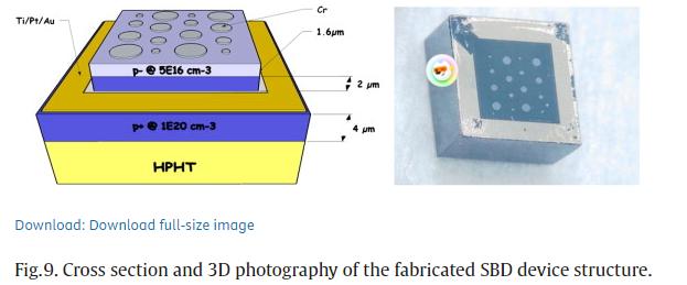
In parallel with the growth of thick heavily boron-doped films, a technology of Schottky diode fabrication, has been developed starting from thin boron-doped films in order to validate Schottky and ohmic contacts. Although a vertically designed diode has been found to be more relevant with regard to the forecased power-devices, the geometry that has been chosen here is that of a pseudo-vertical diode. Indeed, this corresponds to a first attempt in order to optimize our fabrication process of Schottky diodes. In parallel, vertical diodes are being processed and results will be reported elsewhere. On a 3 × 3 × 1.5 mm3 Ib HPHT diamond substrate, a 6 μm-thick heavily doped layer has been grown using a medium MWPD (50 W cm− 3, [B]/[C]gas of 2000 ppm) to achieve the metal-to-semiconductor transition. A second layer has then been deposited in the same reactor choosing growth conditions allowing limiting boron incorporation (a few ppm of [B]/[C]gas and 100 W cm− 3).

A mesa structure of 2×2 mm2 has then been fabricated at the centre of the sample by ICP etching, and Ti/Pt/Au ohmic contacts have been evaporated around the mesa structure on the heavily boron doped layer surface and subsequently annealed at 500 °C for 1 h under nitrogen flow. Circular chromium contacts with different diameters (100 and 150 μm) have finally been deposited on top of the mesa structure in order to obtain Schottky contacts.
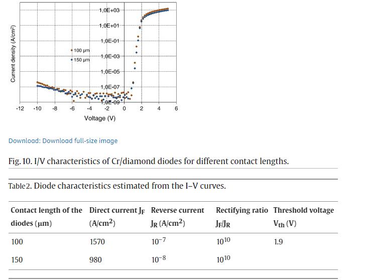
Typical I–V characteristics are presented in Fig. 10 for two diode diameters. From these curves, the main diodes parameters have been estimated (Table 2).

Rectifying ratios as high as 1010, associated with current densities reaching 1500 A cm− 2 are demonstrated. Nevertheless, the reverse current is relatively high when the voltage reaches tens of volts. This behaviour is likely to be related to defects that can have various origins. Bulk defects can induce leakage paths in the material, and near surface homogeneously distributed defects across the contact area can also act electrically as highly doped and low barrier height regions.
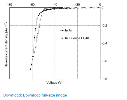
Current–voltage measurements at reverse bias performed with the sample in air or immersed in an insulating liquid (fluorine FC40) are presented in Fig. 11. The insulating liquid avoids electric field crowding at Schottky contact edges causing premature breakdown of the device. A breakdown phenomenon in diamond is observed near − 55 V which corresponds to a breakdown electric field of 1.3 MV cm− 1, if a triangular field distribution within the uniformly doped p− layer is assumed. This value is still below the theoretical predictions for diamond (10 MV/cm) which emphasizes on the challenges still remaining on diamond growth. Nevertheless, these results are very encouraging.
Rectifying ratios as high as 1010, associated with current densities reaching 1500 A cm− 2 are demonstrated. Nevertheless, the reverse current is relatively high when the voltage reaches tens of volts. This behaviour is likely to be related to defects that can have various origins. Bulk defects can induce leakage paths in the material and near surface homogeneously distributed defects across the contact area can also act electrically as highly doped and low barrier height regions.
Current–voltage measurements at reverse bias performed with the sample in air or immersed in an insulating liquid (fluorine FC40) are presented in Fig. 11. The insulating liquid avoids electric field crowding at Schottky contact edges causing premature breakdown of the device. A breakdown phenomenon in diamond is observed near − 55 V which corresponds to a breakdown electric field of 1.3 MV cm− 1, if a triangular field distribution within the uniformly doped p− layer is assumed. This value is still below the theoretical predictions for diamond (10 MV/cm) which emphasizes on the challenges still remaining on diamond growth. Nevertheless, these results are very encouraging.

Schottky diode modeling has shown that only a vertical component geometry can ensure high current operation (higher than 100 A). With such a geometry the on-state resistance (Ron) can be decreased by a factor of 4 to 5. However this implies that the thick (> 100 μm) highly boron doped (1020 cm− 3) diamond films are prepared so that they can mechanically robust to be separated from the substrate which is quite challenging.
The growth of thick films actually requires finding experimental conditions able to achieve high growth rate, high diamond purity and a good surface morphology. These conditions should involve high MWPD. However, above 80 W cm− 3, we have observed a strong reduction in doping efficiency, down to values as low as 0.01, limiting boron incorporation to a few 1019 cm− 3.
Technology for pseudo-vertical Schottky diodes fabrication has been validated showing encouraging I–V characteristics (current density between 1000 and 2000 A cm− 2, a rectifying ratio of 1010 and a breakdown electric field in excess of 1.3 MV cm− 1. This technology is now operational and the next step is the development of a vertical structure starting from the synthesized thick heavily boron doped free-standing films.
The boron-doped single-crystal diamond produced by CSMH can achieve doping from low concentration to high concentration. It has realized a uniform and controllable concentration and a customizable boron doping process.Lightly B-doped diamonds offer excellent carrier mobility, making them ideal substrates for semiconductor applications. Heavily B-doped diamonds provide low electrical resistance, serving as conductive electrodes for ohmic contacts.Furthermore, it is an ideal material for the fabrication of high-temperature, high-power semiconductor components and can also be used in electrochemistry.Additionally, CSMH offers high-quality diamond wafer substrates (e.g., on Si or SiC), enabling customers to develop advanced semiconductor devices.
 闽ICP备2021005558号-1
Leave A Message