With the best overall electronic and thermal properties, single crystal diamond (SCD) is the extreme wide bandgap material that is expected to revolutionize power electronics and radio-frequency electronics in the future. However, turning SCD into useful semiconductors requires overcoming doping challenges, as conventional substitutional doping techniques, such as thermal diffusion and ion implantation, are not easily applicable to SCD. Here we report a simple and easily accessible doping strategy demonstrating that electrically activated, substitutional doping in SCD without inducing graphitization transition or lattice damage can be readily realized with thermal diffusion at relatively low temperatures by using heavily doped Si nanomembranes as a unique dopant carrying medium. Atomistic simulations elucidate a vacancy exchange boron doping mechanism that occurs at the bonded interface between Si and diamond. We further demonstrate selectively doped high voltage diodes and half-wave rectifier circuits using such doped SCD. Our new doping strategy has established a reachable path toward using SCDs for future high voltage power conversion systems and for other novel diamond based electronic devices. The novel doping mechanism may find its critical use in other wide bandgap semiconductors.

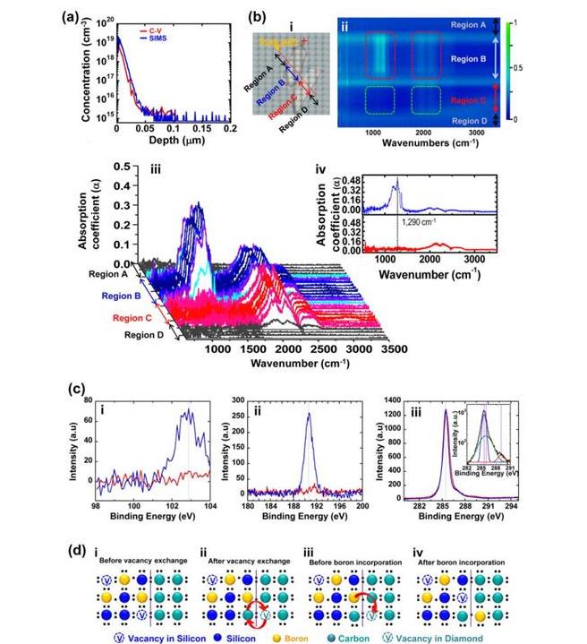
Further characterizations of boron-doped nSCD were performed using Fourier transform infrared spectroscopy (FTIR). Generally, boron inactivation could result from non-substitutional boron sites or aggregated substitutional boron sites. FTIR is an effective method for evaluating the substitutional doping status in a diamond. The FTIR results are shown in Fig. 2(b). Fig. 2(b–i) shows two diamond plates of the same type: one is boron doped (scanning region B) that is realized using the above thermal diffusion method and the other is undoped (scanning region C) as a reference. Figs. 2(b-ii)–(2-iv) show the FTIR mapping results and the scanned spectra. The boron doped diamond shows the characteristic absorption peak at 1290 cm−1, which clearly indicates the electrical activation of boron atoms. In contrast, the peak does not appear in the undoped reference diamond. Since substitutional doping, i.e., boron-carbon sp3 bonding formation, is necessary for electrical activation of doped boron atoms, the FTIR and the C−V characterization results prove the substitutional doping of boron atoms in the nSCD. It should be noted that the characteristic absorption peaks associated with boron interstitials and boron interstitial complexes in diamond can be observed at 1420, 1530, 1570, and 1910 cm−1, but no such peaks appeared in our FTIR spectra.Moreover, the absence of the three infrared B-B cluster absorption peaks (553, 560, and 570 cm−1) indicate that no aggregated substitutional boron sites were formed.The broader peaks, which appear from 1900 to 2300 cm−1 are the inherent two-phonon lines of diamond associated with C−C bonds. They appear in both the boron doped and undoped diamond samples.
X-ray photoelectron spectroscopy (XPS) was performed on both doped diamond and undoped diamond (as a reference). The binding energies for Si1s, B1s and C1s peaks have been identified with constant pass energy of 50 eV and 100 meV energy step as shown in Fig. 2(c). The C–Si peak at ∼103 eV indicates that a chemical reaction between Si and carbon atoms has occurred at the Si–diamond interface (Fig. 2(c-i). However, the absence of an Si peak in the Raman spectrum (Fig. S7) in the range of 400–1200 cm−1 indicates that the C-Si reaction occurred very shallowly (<10 nm) at the diamond surface.43 Boron substitution in diamond yielded a B1s peak at 190.6 eV corresponding to B–C (Fig. 2(c-ii)) confirming that boron doping was successful. This is consistent with the SIMS, C−V, and FTIR analyses. Fig. 2(c–iii) shows the XPS spectra for the core C1s peak in the binding energy region around 280–295 eV for the undoped and boron doped nSCD samples. De-convoluted C1s peaks using the Gaussian/Lorentzian function in the inset of Fig. 2(c-iii) shows a strong sp3 C–C bonding at 285.4 eV and a very small C–O and C = O bonding at 286.4 eV and 287.9 eV, respectively, indicating that the single crystallinity of nSCD was not degraded by the boron diffusion process.
The XPS results obtained above suggest clues for elucidating the boron diffusion doping mechanisms. Especially, the C-Si bonding (Fig. 2(c-i) plays an important role for the observed boron diffusion. First-principles density functional theory (DFT) simulations36,37 were performed to understand the diffusion mechanism. Two mechanisms were proposed to yield enhanced boron diffusion through enhanced vacancies in diamond (detailed calculation can be found in the supplementary material). The first mechanism involves injection of excess vacancies into the diamond from the SiNM, which has a much larger intrinsic vacancy concentration than diamond as well as excess vacancies from ion implantation into the SiNM. DFT calculations verify that this vacancy injection is much more energetically favorable than the usual mechanism for vacancy formation in diamond (movement of carbon to the diamond surface). Fig. 2(d) shows the cartoon illustration of the proposed injection and diffusion mechanism. Besides the above vacancy injection into diamond from Si, excess vacancies can also be additionally created by formation of SiC at the SiNM and diamond interface, which stabilized the vacancies by almost exactly the required 0.7 eV needed to explain the enhanced boron diffusion rate into diamond. Both mechanisms could play a role and further research is required to elucidate their contributions. In each case, diffused boron atoms from Si are expected to immediately become substitutional atoms in diamond if the diamond does not have pre-existing vacancy related defects (ideal situation). Since no vacancy defects are additionally generated in diamond during the diffusion process, a high temperature anneal that is necessary for post-implantation38 then becomes unnecessary in such a doping process.

Based on the identified vacancy exchange mechanism, it is unlikely that boron atoms diffuse to non-substitutional sites, which is different from ion implantation induced case. It is also noted that the realized boron doping concentration in our method is much lower than that realized in synthetic diamond, and therefore the likelihood of forming aggregated boron substitutional sites should be rather small.
Substitutional boron doping in diamond using thermal diffusion has never been considered possible in the past. Our experiment clearly demonstrated the viability of boron doping through the thermal diffusion process using heavily doped, bonded SiNM as dopant carrying medium. The process is also simple and easily accessible. We propose that the origin of the successful doping is enhanced boron diffusion into diamond enabled by the Si-C bonding states near the Si–diamond interface, which lower the energy to create diamond vacancies and enhance boron transport.
The graphitization-free process is thought to be directly related to the intimate bonding between Si and diamond. A previous study has shown that introducing impurities at elevated temperature in diamond can prohibit graphitization during thermal annealing. In the current thermal diffusion experiment, boron atoms accumulate at the bonded surface of the diamond as soon as thermal diffusion begins to occur at an elevated temperature. Therefore, no phase transition is expected to happen at the SiNM bonded diamond surface under the special thermal diffusion setting. This expectation is consistent with experimental observations.
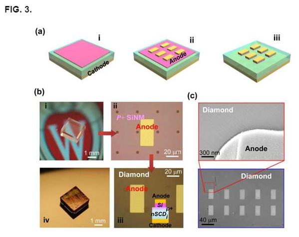
The above boron doping method is used to fabricate diodes using a 2 × 2 mm2, 120 μm thick nSCD plate (Fig. 3). Fig. 3(a) shows the process flow for fabricating vertical p-i junction diodes. After completion of SiNM bonding and boron thermal diffusion from SiNM to diamond (Fig. 1(a-v) the cathode is formed first on the bottom side of the diamond plate. The anode is formed directly on top of the SiNMs (Fig. 1(a-ii)), which previously served as a boron carrying medium, since it is much easier to form ohmic contacts on heavily p-type doped Si. It is noted that a p-i junction is not formed between Si and diamond in this case, but between the p-type doped diamond surface and the intrinsic diamond bulk. Both the anode and the cathode contacts are ohmic contacts. To prove that the p-i junction is formed in diamond not in between Si and diamond, a p-i diamond diode without an SiNM layer, which was removed after completion of boron diffusion, was fabricated. The results are shown in the supplementary material (Fig. S6).43 Fig. 3(b) shows (i) the optical images of the diamond before processing, (ii) the SiNM bonded diamond, (iii) finished diodes, and (iv) the diamond diode array. Fig. 3(c) further shows the scanning electron microscope (SEM) images of the finished diamond diodes. As can be seen here, using the transfer printed and patched SiNMs, selective doping can be easily realized on the diamond surface.
The boron-doped single-crystal diamond produced by CSMH can achieve doping from low concentration to high concentration. It has realized a uniform and controllable concentration and a customizable boron doping process.Lightly B-doped diamonds offer excellent carrier mobility, making them ideal substrates for semiconductor applications. Heavily B-doped diamonds provide low electrical resistance, serving as conductive electrodes for ohmic contacts.Furthermore, it is an ideal material for the fabrication of high-temperature, high-power semiconductor components and can also be used in electrochemistry.Additionally, CSMH offers high-quality diamond wafer substrates (e.g., on Si or SiC), enabling customers to develop advanced semiconductor devices.
 闽ICP备2021005558号-1
Leave A Message