Pos:
Home KnowledgeTechnologyDiamond wafer ,assists solving the packaging problem of high-voltage power devicesIn recent years, the increasing demand for high voltage and high power, as well as the rapid innovation of process technology, have driven the development of power devices towards small size, high performance, and fast speed. It is the trend to achieve modularization through multi chip connections during packaging. But the resulting circuit heat generation also rapidly increases, which will lead to a sharp accumulation of heat generated per unit volume of power module devices, resulting in a decrease in chip lifespan.
Practice has shown that the failure rate of devices caused by the inability to dissipate heat in a timely manner is 55%. The lifespan of gallium arsenide or silicon semiconductor chips is greatly affected by temperature. For every 10 ℃ increase in temperature, the failure caused is 3-5 times that of the original. Because the working temperature of circuits in electronic devices is constantly rising, most of the losses come from thermal radiation. If heat cannot be effectively dissipated, thermal stress and fatigue will occur between materials with mismatched thermal expansion coefficients, leading to the burning of power modules. Therefore, heat dissipation is a crucial issue that cannot be ignored in power electronic devices.
Generally speaking, electronic packaging includes several parts such as interlayer media, framework wiring, sealing materials, and packaging substrates. Metal coatings, chips, and other modules in the packaging system usually have good heat dissipation capabilities. Therefore, the key to affecting the heat dissipation of electronic devices lies in the insulation substrate materials used in the packaging. That is to say, one of the key to solving the problem of device heat dissipation is to choose a suitable packaging substrate.

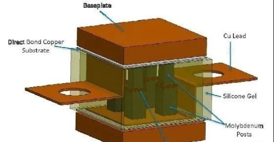
Packaging diagram of power electronic devices
Common electronic packaging substrates include organic packaging substrates, metal and metal matrix composites, and ceramic based packaging substrates.
Organic packaging substrate: As a traditional packaging substrate material, organic packaging substrates have low dielectric constant, light material, are easy to process into fine shaped circuits, are suitable for mass production, and have low manufacturing and packaging costs. However, with the increasing application of high-power and large-scale electronic devices, the packaging requirements for devices are also increasing. Due to the poor electrical performance, low high temperature resistance, poor thermal conductivity, and low compatibility with the thermal expansion coefficient of the chip, organic packaging substrates are no longer able to meet the packaging requirements of power electronic devices, and are particularly unsuitable for packaging products with high airtightness and high pressure and high temperature resistance in fields such as military engineering, smart grids, aircraft, and high-speed rail.
Metal and metal matrix composite packaging substrates: Insulating metal substrates have been successfully developed and used in electronic packaging due to their high thermal conductivity, high mechanical strength, excellent conductivity, ductility, and good processing performance. Aluminum based composite materials are commonly used substrates in metal based packaging, with advantages such as high specific stiffness and strength, low density, and easily adjustable thermal expansion coefficient. They have been widely used in industries such as power LEDs, power electronic devices, aerospace, and hybrid integrated circuits. Although metal materials have many advantages, they need to be improved in terms of wear resistance, corrosion resistance, high temperature resistance, high stress at the solid crystal interface, and easy cracking, and the production cost of metal substrates is relatively high.
Ceramic based packaging substrates: Currently, commonly used ceramic based packaging substrates include Al2O3, BeO, SiC, AlN, Si3N4, etc. However, the thermal expansion coefficient and dielectric constant of Al2O3 are relatively high compared to Si single crystals, and the thermal conductivity is still not high enough, which makes Al2O3 ceramic substrates unsuitable for use in high-frequency, high-power, and ultra large scale integrated circuits. The thermal conductivity of SiC ceramics is high, and the higher the purity of SiC crystals, the greater the thermal conductivity. The biggest drawback of SiC is its high dielectric constant and low dielectric strength, which limits its high-frequency applications and is only suitable for low-density packaging. AlN material has excellent dielectric properties and stable chemical properties, especially its thermal expansion coefficient that matches silicon, making it a promising semiconductor packaging substrate material. However, the current highest thermal conductivity is only 260W/(m · K). With the increasing demand for heat dissipation, AlN material also faces certain development bottlenecks. Diamond is currently known to have the highest thermal conductivity in nature. The thermal conductivity of single crystal diamond is 2200-2600 W/(m.K), with a thermal expansion coefficient of about 1.1 × 10⁻⁶/℃. It has excellent properties in semiconductors, optics, and other fields that other packaging materials cannot achieve.

CSMH is a high-tech company specializing in the research and development, production, and sales of diamond wide bandgap materials. Its products include diamond wafer Ra<1nm, diamond heat sink thermal conductivity 1000-2000W/m.k, diamond optical windows, diamond heterojunction integrated composite substrates, AlN thin films, and more. CSMH is committed to solving the thermal management problems of high-power devices in various industries and has been recognized by professional customers in fields such as high-speed rail, lasers, 5G communication, new energy vehicles, and new energy photovoltaics.
 闽ICP备2021005558号-1
Leave A Message