Pos:
Home KnowledgeTechnologyResearch on GaN Heat Dissipation Technology for Diamond Wafer SubstratesThe technical difficulties of diamond based GaN devices lie in the interface thermal resistance, lattice mismatch, thermal stress, and low thermal conductivity of nanocrystalline diamond grown by CVD. CVD growth generally occurs at 700-800 degrees Celsius, due to the difference in thermal expansion coefficients between GaN and diamond. When the device is cooled to room temperature, there will be significant thermal stress at the interface, causing the device to fracture. Growing diamond on GaN requires a protective layer, which increases the interfacial thermal resistance and greatly reduces the heat dissipation efficiency of the diamond. Moreover, the diamond grown by CVD is nanocrystalline near the interface, with a very low thermal conductivity of only a few tens of W/m · K. After several micrometers of CVD growth, the thermal conductivity of polycrystalline diamond will increase to approach that of bulk materials, and this low-quality diamond layer will also hinder the heat dissipation of GaN devices.
Therefore, how to use diamond as a heat sink or substrate for GaN based power devices has become a current research hotspot. At present, various technical forms have been reported, including polycrystalline diamond substrate GaN heat dissipation technology, single crystal diamond substrate heat dissipation technology, high thermal conductivity diamond passivation layer heat dissipation technology, etc.
1. Heat dissipation technology of polycrystalline diamond substrate GaN
(1) Low temperature bonding technology
Bonding technology is an important technology in the manufacturing process of the semiconductor industry. The vast majority of electronic materials, electronic device structures, and other connections are applied to bonding technology, which can be divided into two categories: high-temperature bonding and low-temperature bonding
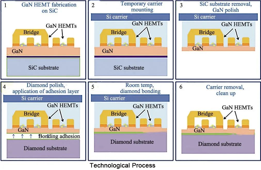
The basic idea of low-temperature bonding is to peel off the GaN epitaxial layer from the original Si substrate, and then add an intermediate layer on the exposed GaN surface to combine with the polycrystalline diamond substrate, so that the active region of the GaN based device contacts the CVD diamond substrate and reduces the junction temperature of the power device.

Low temperature bonding technology of GaN on diamond substrate
(2) Direct growth of diamond on the back of GaN epitaxial layer
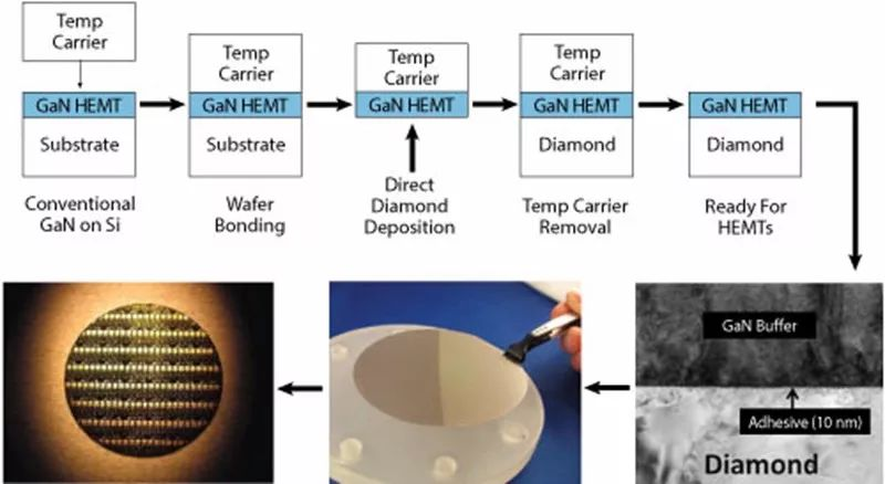
Another method for preparing diamond based GaN devices, different from low-temperature bonding technology, is to remove the substrate and part of the GaN buffer layer, and then deposit a dielectric layer on the back of the epitaxial layer to protect the GaN epitaxial layer before depositing the diamond substrate (thickness~100 μ m) .

The production process of GaN on diamond crystal wafers
2. Epitaxial GaN on Single Crystal Diamond Substrate
With the continuous development and improvement of single crystal diamond preparation technology, direct epitaxial growth of GaN wafers on single crystal diamond substrates has also been used to improve heat dissipation requirements.
Although heteroepitaxy of AINGaN/GaNHEMTs can currently be achieved, the difficulty is great. Due to the cubic structure of diamond and the hexagonal wurtzite structure of GaN, the difference in crystal structure makes it extremely difficult to epitaxial GaN on single crystal diamond. In addition, the huge difference in lattice constant and thermal expansion coefficient between GaN and diamond also poses great difficulties for preparation. In addition, the limitations of single crystal size and cost further affect its application
3. High thermal conductivity diamond passivation layer heat dissipation technology
M. from Germany Seelman Eggbert explored the use of high thermal conductivity diamond passivation layers for thermal diffusion on GaN FETs from both theoretical and experimental perspectives. The compatibility between GaN FETs process conditions and low-temperature diamond deposition was discussed in detail, and a selective low-temperature (deposition temperature of 400 ℃) method was used to grow diamond films by depositing 0.7 on the gate of GaN FETs μ The output and transmission characteristics of transistors before and after depositing diamond films with a thickness of m show no significant changes. It is believed that this is the first time that diamond can be directly deposited on III-V semiconductor transistor devices for thermal diffusion, but the specific cooling effect of diamond has not been verified.
Although the high thermal conductivity diamond passivation layer heat dissipation technology has great potential, the deposition of nano diamond films in the production of HEMTs is often limited by the device process conditions, the deposition temperature is generally low, and the thermal conductivity of nano diamond films is not high, all of which limit the application and promotion of this technology

CSMH is committed to the production and research of diamond semiconductor materials. It uses the MPCVD method to prepare 1-4 inch diamond wafers, with a surface roughness of Ra<1nm and a thermal conductivity of 1000-2000W/(m · K), which basically meets the basic requirements for size, thermal conductivity, surface smoothness, and surface shape with semiconductor materials such as Si, GaN, lnP, and Ga2O3.
 闽ICP备2021005558号-1
Leave A Message