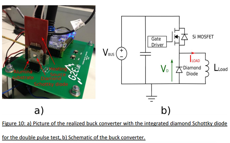
Wide bandgap (WBG) semiconductors have been used since several years to improve performances of power electronics converters. Materials such as silicon carbide (SiC) or gallium nitride (GaN) allow power converters to operate at higher voltages, higher temperatures, and higher switching frequencies than silicon (Si). These benefits are offered by the superiorities of the WBG materials. Among WBG semiconductors, diamond is the most promising material for power electronics applications. Whereas experimental benefits of SiC and GaN devices in actual power converters have been widely demonstrated, the system level benefits of diamond power devices have not been yet clearly described. This article will offer a system level benchmark of diamond devices in power converters, based on the characteristics of fabricated diamond Schottky diodes, their implementation in power converters and a theoretical benchmark versus SiC power devices. The physical properties of diamond such as a high electric field (10 MV/cm), a high hole mobility (1300 cm2/(V.s)) make it the most suitable semiconductor for high power converters. These values are calculated at room temperature for a 1 kV breakdown voltage with a 1.6x1017 cm-3 doping level for the required drift region. These properties combined with a high thermal conductivity (22 W/(cm.K)) and a very low intrinsic carrier concentration at room temperature (2.2x10⁻²⁷ cm-3) lead to the highest figures of merit (FOM), higher than SiC or GaN materials.
Considering the diamond devices, further works are still required to bring such attractive devices in power converters. The first main improvements are the developments of devices with larger areas, with the reduction of defect densities and perfect control of diamond surface quality over a wide area. The increase of diamond “wafer” size is desired and expected but even with 5 mm x 5 mm diamond substrates, there is a possibility to fabricate in a first development
step diamond devices with current ratings higher than 100A. Moreover, some studies are done on heteroepitaxially grown diamond substrates. The parallelization of diamond devices, considering both the NTC and PTC coefficients and the use of higher thermal resistances must be investigated. A first step towards parallelization of diamond devices has been presented in [46]. The second improvements on the diamond devices are the required solutions to increase theelectric field during the off-state. Indeed, reaching higher electric field, closer to the theoretical 1D breakdown, will help to increase the doping level of the drift layer and therefore reducing even further the on-state losses. Innovative solutions have been proposed for diamond junction terminations, which must be further investigated and fabricated.

CSMH has been committed to the research and development and production of diamond materials. Now it has products such as diamond heat sink sheet,diamond wafer, diamond window to provide customers with a comprehensive thermal management solution.
 闽ICP备2021005558号-1
Leave A Message