Pos:
Home KnowledgeTechnologyDiamond wafer as the heat spreader for the thermal dissipation of GaN-based electronic devicesBenefitted from the high breakdown voltages (10 times higher than Si), high switching speed (over GHz), compact size, and tunable electronic architecture, III-V nitride semiconductor is becoming one of the best candidates for high-power electronics to enable the increasing power density and high conversion efficiency. The commercialized AlGaN/GaN high electron mobility transistors (HEMTs) have led to the entry into the mediumpower market, and play a central role for the RF and millimeter-wave applications. In the applications of 5G communications, radar, and electronic warfare, the HEMTs devices can offer more than 10 times higher power density than the existing Si technologies.
This giant power induces a huge amount of heat in the chip area, creating localized hot spots with fluxes above 10 kW/cm2 and package-level volumetric heat generation that can exceed 100W/cm−3. The high-level power dissipation results in the challenges using conventional approaches for the thermal management. With the increased power density, self-heating inside the devices becomes an essential issue that accelerates the failure and poor reliability in the real application. Thermal dissipation through conventionally used approaches is no longer adequate. To achieve the effective thermal dissipation, the heat spreader with a much higher thermal conductivity is required.The current GaN wafers are typically grown on sapphie, silicon (Si), silicon carbide (SiC), or free-standing GaN substrates, whose thermal conductivities are 35, 150, 400, and 280W/mK, respectively, which are far from the requirements. The ideal heat spreader would be a substrate that is both highly thermally conductive and electrically insulating. Diamond, with the thermal conductivity up to 2400W/mK at room temperature for the single crystals, and approaching 2000W/mK for the polycrystals, is the best candidate as a heat spreader for GaN power transistors. Early simulations and modelling showed that the passive thermal extraction by direct contact with diamond could dramatically reduce junction temperatures by 25-50%. However, as shown in Table 1, diamond and GaN exhibit widely mismatched properties, such as the crystalline structures, lattice constants and thermal expansion coefficients (TEC), making them challenging as bonded or growth pairs.
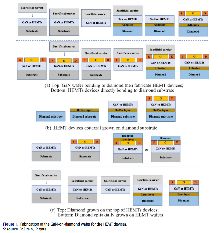
Over the past twenty years, a variety of methods have been developed to utilize diamond as the heat spreader for AlGaN/GaN power transistors. The developed wafer is therefore called “GaN-on-diamond wafer”. The approaches are summarized in Figure 1, which include: (1) bonding of diamond to GaN wafers or directly to the HEMT devices with/without an adhesion layer, (2) GaN epitaxial growth on single-crystal or poly-crystal diamond substrate, then fabrication of HEMT devices, and (3) nanocrystalline or poly-crystalline diamond growth on the frontside or backside of GaN or the HEMTs devices. For the three approaches, the thermal resistance at the GaN/diamond, which is referred to the “effective thermal boundary resistance (TBReff)”, is one of the factors that significantly increases the overall temperatures during device operation. Therefore, the optimizations on the integration technique and interface property are important. In this review, the state-of-the-art development on the GaN-on-diamond wafer and the modified fabrication process for HEMTs with regard to different integration methods will be presented. The strategies to improve the interfaces and reduce the TBReff will be summarized and discussed. The device performances will be further shown with respect to different methods.

CSMH has been committed to the research and development and production of diamond materials. Now it has products such as diamond heat sink sheet,diamond wafer, diamond window to provide customers with a comprehensive thermal management solution.
 闽ICP备2021005558号-1
Leave A Message