Gallium nitride (GaN) is a wide bandgap compound III-V semiconductor with high breakdown electric field, high electron mobility, and high electron saturation velocity that translate in a tremendous potential for high power and high frequency applications.
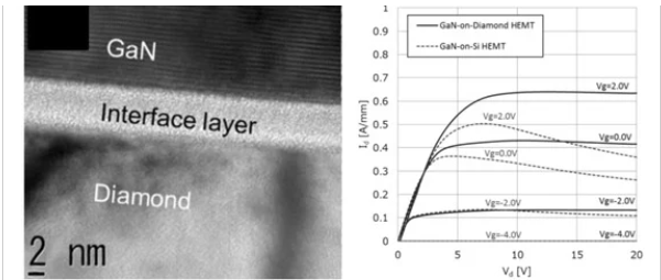
The capability of efficiently transferring the heat away from the localized hotspots and the consequent control of the device temperature is fundamental to achieve high levels of stability and reliability in HEMT applications. Diamond has the highest thermal conductivity (κ) of any bulk material, and the integration of diamond films and GaN HEMTs as substrates or packaging has already proven to enhance the extraction of the heat generated during the devices operation, leading to a substantial decrease in the junction temperature as well as to an increase in the maximum power density the HEMTs can safely handle. Diamond has been successfully integrated with HEMT devices following different approaches.
The integration of diamond and GaN for the fabrication of HEMTs with superior thermal handling capability has been an active research topic involving academic and industrial institutions for more than 20 years. Generally speaking, the integration of both materials can be done in two ways: replacing the GaN substrate with diamond or placing the diamond on top of the device, close to the gate hotspot.
The fabrication of GaN-on-diamond wafers can be made using three fundamentally different approaches: (i) depositing diamond films by CVD directly on the back of GaN wafers, following the substrate removal (hereafter referred to as GaN-on-diamond); (ii) bonding GaN HEMT wafers and diamond substrates (bonded wafers); and (iii) growing the epitaxial GaN layers directly on diamond substrates (GaN epitaxy). Placing the diamond on top of the HEMT device can be done simply by growing the diamond films directly on the passivated surface of the device (capping diamond).

The integration of diamond and GaN devices has been an active research topic for 20 years. The involvement of companies like Fujitsu and Mitsubishi, for instance, is representative of the impact that hybrid GaN/diamond electronic devices can have on some applications.
Generally speaking, the fabrication of diamond-on-GaN wafers by direct diamond CVD on the back of the GaN wafers has been quite successful and commercial RF power amplifiers fabricated on GaN-on-diamond wafers are currently available for satellite communications. Recent advances in the epitaxial growth of GaN layers on PCD substrates anticipate interesting technological developments in a near future. Far from having reached the limits of the technology, it can be thus said that the integration of diamond and GaN will remain an active research topic in the years to come, involving academic and industrial players, with the ultimate goal of increasing the power density and reliability of GaN HEMTs.
CSMH has made breakthroughs in GaN & Diamond combination solutions: GaN on Diamond, Diamond on GaN, and GaN & Diamond bonding. Among them, the required diamond wafer’s performance has proved to a level with Ra<1nm(even<0.5nm), contributing to improve the success rate of diamond and GaN bonding.
 闽ICP备2021005558号-1
Leave A Message