Pos:
Home KnowledgeTechnologyElectrical and Thermal Performance of AlGaN/GaN HEMTs on Diamond Substrate for RF ApplicationsAlGaN/GaN high electron mobility transistors (HEMTs) on SiC substrates have been reported with extremely high RF power densities reaching 40 W/mm . Such capabilities of AlGaN/GaN heterostructure, however, cannot be exploited for real applications without developing aggressive and novel thermal management techniques to control the channel temperatures so that the devices can operate reliably. To address the problem and make use of untapped RF power of GaN, we have been investigating AlGaN/GaN HEMTs on high thermal conductivity polycrystalline diamond substrates.
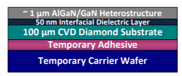
To prepare the GaN-on-diamond device wafers, the AlGaN/GaN HEMT layer structure was first grown by metal-organic chemical vapor deposition (MOCVD) on a high resistivity Si (111) substrate. Device wafers were then prepared by first removing the host Si (111) and transition layers beneath the AlGaN/GaN epitaxy, depositing a 50 nm thick proprietary dielectric onto the exposed AlGaN/GaN, and finally growing 100 µm-thick polycrystalline diamond using a chemical vapor deposition (CVD) process onto the dielectric adhered to the epitaxial AlGaN/GaN films. GaN-on-diamond wafers were temporarily mounted on the carrier wafers for device processing. Using the contactless Lehighton measurement, an average sheet resistance of 440 Ω/ϒ was measured on the wafers. HEMTs were fabricated using a dielectrically defined 0.25 µm gate-length process. HEMT fabrication steps included mesa isolation, Ohmic contacts, gate process, dielectric passivation and overlay metallization. Source-drain spacing of 4 µm was used. Test HEMTs with gate peripheries from 50 µm to 200 µm and Transfer Length Measurement (TLM) test structures were fabricated for electrical and thermal characterization.

DC characteristics of the test HEMTs were measured using an Agilent Semiconductor Parameter Analyzer. Current-voltage (I-V) curves of a 50 µm gate width HEMT up to a high drain voltage of 40 V, show promising and robust drain current characteristics along with a maximum current density of 1 A/mm.
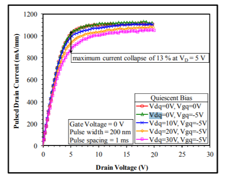
Pulsed I-V tests were performed using DIVA test set up to evaluate current collapse (CC) in the fabricated devices. The picture below shows the measured pulsed I-V of a 2x100 µm HEMT. It can be seen that the device did not show any CC when pulsed from a pinched-off state of Vgq = -5 V while Vdq = 0 V. CC increases with Vdq. However, even at a maximum Vdq of 30 V, CC is only 13 % which is comparable to that of standard GaN-on-SiC devices. These results are promising for good RF performance of these devices.

Small signal s-parameters of 2 x100 µm HEMTs were measured using Agilent 8510C network analyzer. Devices reach over 7 W/mm output power at 40 V bias, which is a record performance for GaN-ondiamond HEMTs at 10 GHz. This is achieved with over 46 % power-added efficiency (PAE). At 28 V, an output power of over 5 W/mm along with the PAE of about 55 % is achieved. The output power achieved in these devices is comparable to that of standard GaN-on-SiC HEMT. PAE of these GaN-on-diamond HEMTs is affected by high gate leakage current, and significant improvement in PAE is expected by leakage reduction.
Thermal performance evaluation of GaN-on-diamond devices was done using micro-Raman spectroscopy and IR thermography techniques. It is determined by micro-Raman analysis that for the same power dissipation the GaN-on-diamond HEMT shows over 25% lower temperature rise than that of GaN-on-SiC. This is a significant improvement, which is attributed to the thermal resistance reduction of GaN on-diamond by means of high thermal conductivity of diamond in the close vicinity (~1 µm) of the hot GaN HEMT junction and removal of defective transition layer of GaN-on-Si beneath the AlGaN/GaN films.
Device wafers have been developed by removing the host Si (111) substrate and transitions layers of GaN-on-Si wafer and subsequently depositing 50 nm dielectric and 100 µm thick CVD diamond layer. Very promising DC characteristics are achieved for HEMTs with maximum current densities in excess of 1 A/mm and operation up to 40 V. Further development is needed to improve the gate leakage current. These devices achieve a record RF power for GaN-on-diamond HEMTs at 10 GHz. Significant improvement of PAE is expected with reduction of leakage current. Further, thermal measurements confirmed over 25 % lower channel temperature rise for GaN-ondiamond HEMTs compared to a standard GaN-on-SiC HEMTs at a fixed power dissipation condition. This significant improvement shows the promise that GaN-ondiamond approach holds for advancing the GaN technology to significantly higher power levels.
As a wide bandgap semiconductor material company, CSMH has professional R&D engineers, large-scale manufacturing capacity and professional and efficient tech support. Now we have products like diamond heat sink, diamond wafer and GaN&Diamond.
 闽ICP备2021005558号-1
Leave A Message