Pos:
Home KnowledgeTechnologyDiamond wafer substrate and InP are bonded under atmospheric conditions to achieve efficient heat dissipationCommunications and networking specialists have been working on THz monolithic integrated circuits (TMIC) with InP high electron mobility transistors (HEMTs) and heterojunction bipolar transistors (HBTs). The direct bandgap of InP is useful in photonic device applications, such as InP laser/modulator/photodetector systems for next-generation optical communications. Accompanying the demand for miniaturization and high-power operation, the power density of these devices has drastically increased. Consequently, InP-based electronic devices suffer from heat dissipation problems due to the low thermal conductivity of 68 W/m/K (Si: 130 W/m/K).For efficient heat dissipation, semiconductor researchers have developed an integration technique for devices on a diamond heat spreader, which has the highest thermal conductivity amongst solid materials (2200 W/m/K).
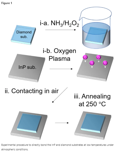
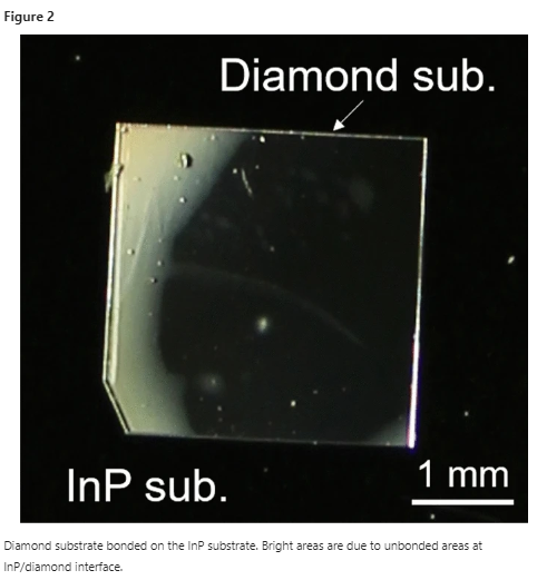
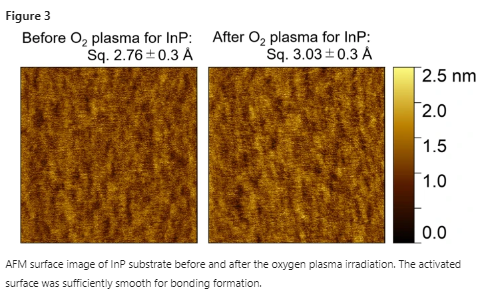
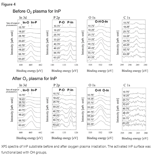
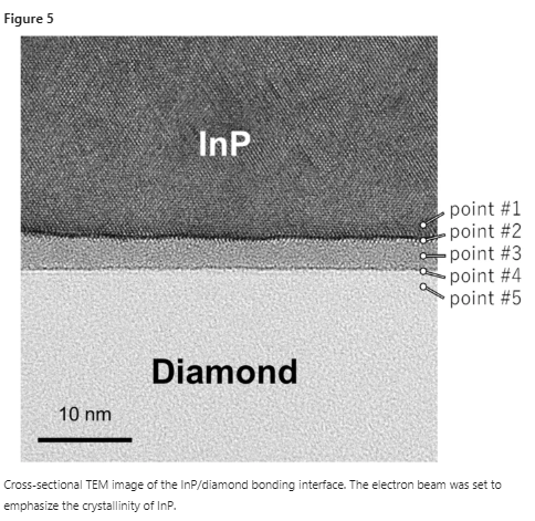
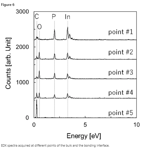
An InP substrate was directly bonded on a diamond heat spreader for efficient heat dissipation. The InP surface activated by oxygen plasma and the diamond surface cleaned with an NH3/H2O2 mixture were contacted under atmospheric conditions. Subsequently, the InP/diamond specimen was annealed at 250 °C to form direct bonding. The InP and diamond substrates formed atomic bonds with a shear strength of 9.3 MPa through an amorphous intermediate layer with a thickness of 3 nm. As advanced thermal management can be provided by typical surface cleaning processes followed by low-temperature annealing, the proposed bonding method would facilitate next-generation InP devices, such as transistors for high-frequency and high-power operations.
Since advanced thermal management can be achieved through simple programs, this bonding technology will help future InP devices with higher integration and power density to achieve efficient heat dissipation.
CSMH focuses on the research and production of diamond wafers. At present, it has diamond wafers, diamond heat sinks, GaN on diamond, AlN on diamond and other products. Among them, high-power semiconductor lasers packaged by diamond heat sinks have been used in optical communications. In the fields of laser diodes, power transistors, and electronic packaging materials, it can provide customers with diamond thermal management solutions.
 闽ICP备2021005558号-1
Leave A Message