Diamond, with its ultra-wideband gap, high dielectric breakdown strength, and high carrier mobility, is known as the ultimate semiconductor in the industry, laying a material foundation for the development of a new generation of semiconductor devices serving in extreme environments such as high temperature and high pressure. Doping is a common method to regulate the conductivity of semiconductors. However, as a recognized top problem in this industry, the efficient doping of diamond is still a bottleneck restricting its commercialization. As another way to regulate the conductivity of semiconductors, strain engineering is to change the electronic band structure of the material by applying lattice strain to the material, thereby regulating its carrier mobility. However, diamond lacks successful practice due to its ultra-high hardness and brittleness. In response to this problem, researcher Dang Chaoqun realized the uniform elastic strain of diamond up to 10 % based on micro-nano mechanics technology, and found the law of regulating the electronic band structure of diamond through strain engineering, which opened up a new idea for promoting the application of microelectronic devices with wide band gap semiconductor materials.
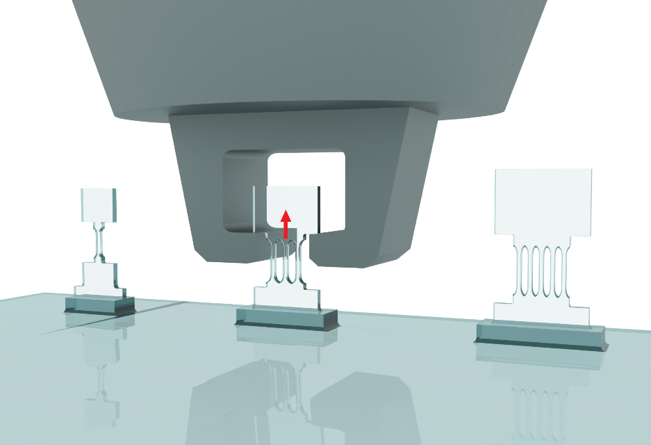
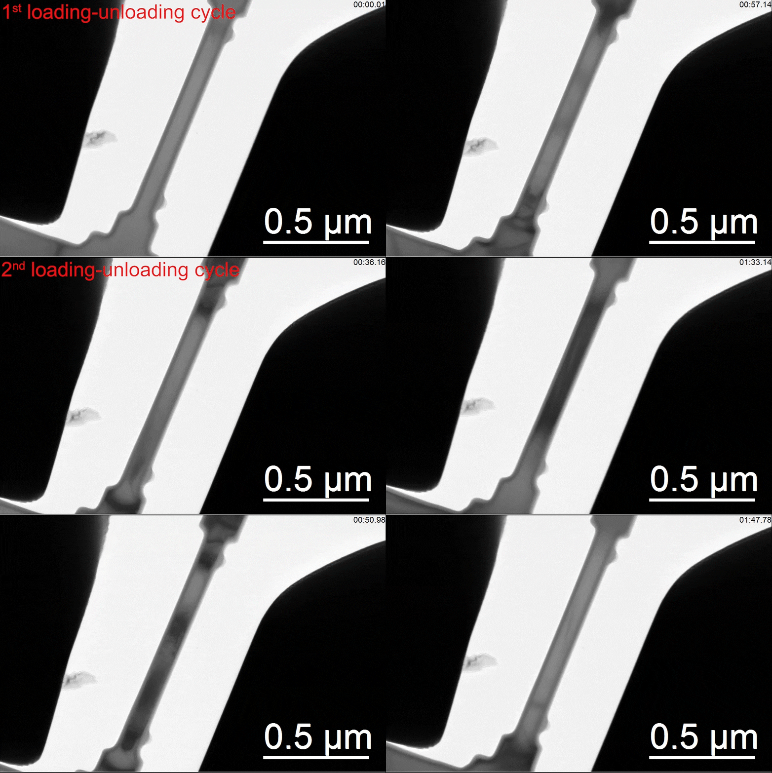
Diamond is not only the hardest material in nature, but is also an extreme electronic material with an ultrawide bandgap, exceptional carrier mobilities, and thermal conductivity. Straining diamond can push such extreme figures of merit for device applications. Dang Chaoqun and her team microfabricated single-crystalline diamond bridge structures with ~1 micrometer length by ~100 nanometer width and achieved sample-wide uniform elastic strains under uniaxial tensile loading along the [100], [101], and [111] directions at room temperature. They also demonstrated deep elastic straining of diamond microbridge arrays. The ultralarge, highly controllable elastic strains can fundamentally change the bulk band structures of diamond, including a substantial calculated bandgap reduction as much as ~2 electron volts. Their demonstration highlights the immense application potential of deep elastic strain engineering for photonics, electronics, and quantum information technologies.

Fig. |Diagram of tensile strain test for diamond microbridge and array samples.

Fig. |The uniform elastic tensile strain of diamond is 7.5 %.

Fig. | Dynamic concept diagram of strained diamond device
CSMH focuses on the research and production of diamond wafers. At present, it has diamond wafers, diamond heat sinks, GaN on diamond, AlN on diamond and other products. Among them, high-power semiconductor lasers packaged by diamond heat sinks have been used in optical communications. In the fields of laser diodes, power transistors, and electronic packaging materials, it can provide customers with diamond thermal management solutions.
 闽ICP备2021005558号-1
Leave A Message