Pos:
Home KnowledgeTechnologySemiconductor application and elastic strain engineering of single crystal diamond waferIn recent years, with the increasing demand for broadband gap semiconductors, the arrival of 5G or even 6G networks, and the demand for high-power high-frequency electrical equipment, traditional silicon-based semiconductor technology faces enormous challenges due to limited performance. As an ultra-wideband gap semiconductor, diamond has become an ideal material for the next generation of microelectronics and photonics due to its many advantages such as ultra-high carrier mobility, thermal conductivity, low thermal expansion coefficient and ultra-high breakdown voltage compared with traditional semiconductors. However, the practical application of diamond in the next generation of electronic products also faces various challenges. A lot of efforts have been made in the experimental modeling and fabrication of diamond high voltage switching diodes, high power high frequency field effect transistor, high temperature devices and MEMS / NEMS. There are defects in the production of diamond wafers, and large-area wafer growth cannot be achieved. Although diamond films with a diameter of 4 inches have been grown on metal iridium substrates in recent years, defects must be further minimized. At the same time, the size of homoepitaxial diamond is also increasing. Therefore, in the near future, large-area and high-quality diamond wafer fabrication can be achieved by updating manufacturing equipment and improving homogeneous / heterogeneous epitaxial growth technology.
The research group of Professor Lu Yang from City University of Hong Kong systematically summarized and prospected the semiconductor application potential of diamond ( synthetic diamond ) and the new opportunities brought by ' elastic strain engineering ' at micro-nano scale. In this paper, the efforts of academia and industry on high-voltage switching diodes, high-power high-frequency field-effect transistors, micro / nano electromechanical systems and devices working at high temperatures based on diamond experimental modeling and construction are reviewed. Some positive progress in solving the large-scale application of diamond devices is discussed, and the preparation requirements of high-quality chemical vapor deposition ( CVD ) large-size single crystal diamond films and the challenges of single crystal diamond doping in electronic applications are emphasized. It further demonstrates the new potential solutions of the research group in recent years to regulate the electronic and photoelectric properties of diamond by actively using the ' elastic strain engineering ' strategy brought by micromachining and micro-nano scale effects, which is expected to provide a new perspective and inspiration for the future development of microelectronics and optoelectronic devices based on single crystal diamond. In addition, there is a shallow doping problem in diamond. The synthesis and application of boron-doped p-type diamond have been relatively mature, and the impurity level and carrier transport characteristics can be well controlled by ion implantation or CVD methods. However, the synthesis of n-type diamond is still very difficult and limits the application of diamond semiconductor materials in the electronic field. It is worth further study in improving doping technology, increasing electron mobility and reducing resistivity.
On the other hand, elastic strain engineering is considered to be a potential method to adjust the electronic properties of diamond, but this method has long been considered impossible due to the inherent ultra-high hardness and brittleness of diamond. Nowadays, with the development of micro-nano technology, it was first reported in 2018 that ultra-large elastic strain was realized in diamond nanostructures. Subsequently, it was predicted by first-principles theoretical calculations that ultra-large elastic strain can change the band gap of diamond. Recently, researchers have further demonstrated that the micro-array structure is obtained by micro-machining single crystal diamond, and the ultra-large and uniform global elastic strain is achieved by pure mechanical loading, which makes the ' deep elastic strain engineering ' of diamond possible. In theory, when extreme strain values are applied, it is even possible to achieve ' metallization ' in diamond, and even diamond can even become superconductors through composite compression-shear deformation. These exciting theoretical predictions open up the possibility of developing new optoelectronic and even quantum devices based on ' strained diamond ' in the future.
As a quantum material that has attracted much attention at present, it has been found that the diamond single quantum system can be controlled by applying stress and strain, which is different from the traditional established method based on electromagnetic field. For example, strain has been used to transfer information between remote quantum systems and to cool a mechanical oscillator to its quantum ground state, opening up new prospects for quantum information processing applications.

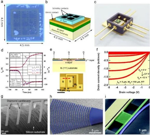
Fig.1.Representative diamond functional devices. ( a, b ) photos and schematics of diamond Schottky diodes ; ( c ) Diamond Schottky diodes for metal / ceramic devices with high-temperature turn-off function ; ( d ) Switching characteristics of diamond Schottky diodes at 50, 150 and 250 °C ; ( e ) Top view and cross section diagram of diamond metal-oxide semiconductor field effect transistor. S, D and G represent source, drain and gate contacts, respectively. ( f ) The relationship between drain current and drain voltage of diamond metal-oxide semiconductor field effect transistor at room temperature ; ( g ) Scanning electron micrographs of diamond devices with multiple cantilevers on silicon substrates ; ( h ) Scanning electron microscopy images of the focused grating coupler ; ( i ) Scanning electron microscopy images of independent diamond resonators in electro-optic mechanical devices.

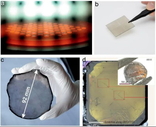
Fig.2.Preparation and progress of new diamond. ( a ) Single crystal diamond was grown on 70 3.5 × 3.5 mm2 HPHT seeds by microwave plasma assisted CVD. ( b ) CVD horizontally connected mosaic wafer ( 40 × 40 mm2 ) ; ( c ) A 155-carat single crystal diamond with a thickness of 1.6 ± 0.25 mm and a diameter of 90 mm was grown on Ir / YSZ / Si ( 001 ) substrate by microwave plasma CVD. ( d ) An amorphous carbon material with semiconductor properties ( band gap of 1.5-2.2 eV ) prepared at high temperature and high pressure with hardness comparable to diamond.

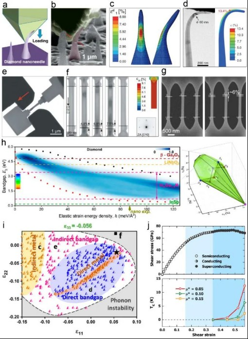
Fig.3. ' Elastic strain engineering ' of single crystal diamond. ( a-c ) Diamond nanoneedle ' push-turn ' deformation diagram, the maximum deformation diagram before fracture and the corresponding finite element simulation reproduce the geometric shape of the nanoneedle bending showing the local elastic maximum principal strain ; ( d ) The single crystal diamond nanoneedles processed by FIB along the [ 100 ] direction were subjected to the ' pressure turning ' deformation test, the maximum bending deformation diagram before fracture and the corresponding finite element simulation to replicate the shape of the nanoneedles and the distribution of the maximum principal strain. The uniaxial tensile device, loading-unloading test and corresponding finite element simulation of ( e, f ) diamond bridge reproduce the longitudinal distribution of elastic strain of diamond bridge. ( g ) The tensile deformation of diamond arrays with multiple bridges simultaneously reaches a maximum tensile strain of 6 % ; ( h ) The band gap of diamond is extended to the semiconductor region ; ( i ) ε11-ε22 strain space shows the direct metal strain region ( brown ) in the direct band gap strain region ( blue ) and the indirect metal strain region ( brown ) in the non-zero indirect band gap strain region ( white region with red symbol ) ; ( j ) With the increase of compression-shear strain, the band gap of diamond evolves into three stages of semi-conductivity, conductivity and superconductivity, and the relationship between critical temperature Tc and strain in the selected range of Coulomb pseudopotential μ *.
As a dedicated research and development, production and sales of wide band gap semiconductor materials, CSMH is committed to becoming the world's leading wide band gap semiconductor material company. The latest Single crystal diamond launched by CSMH has high thermal conductivity of up to 2000W·(m·K), optical transmittance of 71.6%, and excellent electronic properties. In addition, there are also core products Polycrystalline diamond (Diamond Heat Sink, GaN on Diamond), and AlN thin film (AIN on Diamond, AIN on Silicon and AIN on Sapphire) and other products can be used in 5G base stations, lasers, medical instruments, high-power LED, new energy vehicles, new energy photovoltaic, aerospace, national defense and other fields.
 闽ICP备2021005558号-1
Leave A Message