The GaN-on-diamond concept was initially introduced in 2003. The original idea relied on the deposition of the PCD film directly on the back of the GaN layer. The first GaN-on-diamond wafer pieces were produced in 2004 by etching the Si substrate of a GaN wafer initially deposited by MOCVD, followed by depositing a 50 nm-thick dielectric layer and then by growing a 25 um-thick PCD film by hot filament CVD (HFCVD). The PCD was deposited on the Ga-face, leaving behind an N-face GaN-on-diamond wafer after the etching of the temporary Si carrier. The fabrication process remains fundamentally the same till today and is represented in Figure 2. The required steps involved (i) performing the GaN epitaxy on a Si substrate, (ii) bonding the GaN HEMT epilayers onto a temporary Si carrier, (iii) etching away the original host Si substrate, (iv) depositing a 50 nm-thick layer of SiN onto the exposed rear face of the GaN, and (v) depositing a 25 um-thick PCD film by HECVD onto the dielectric, Finally, by (vi) removing the temporary Si carrier. afree-standing GaN-on-diamond wafer was obtained.

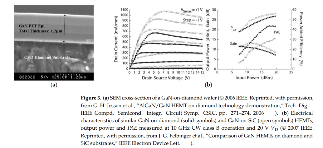
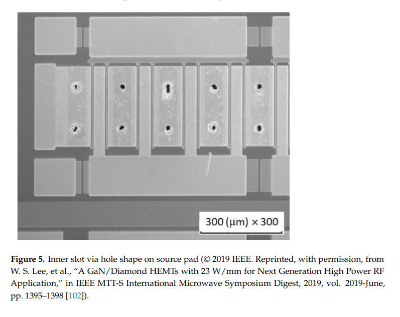
By 2006, the process had been optimized to fabricate a Ga-face (i.e., right side upGaN-on-Diamond HEMT epitaxial wafer and the operation of an AlGaN/GaN HEMT with a 25 um-thick PCD film located 1.2 um below the electron channel was reported . The scanning electron microscope (SEM) cross-section of the GaN-on-diamond wafer is shown in Figure 3a. These first unpassivated HEMTs had a high contact resistance that translated in low current capability (maximum drain current ID max = 306 mA/mm) and low peak transconductance (gm peak = 70 mS/mm). Further iterations improved the performance of the HEMTs, nevertheless, and in spite of having half the thermal resistance Ru of GaN-on-SiC HEMTs (6 against 12 K·mm/W,respectively), in 2007 GaN-on-diamond HEMTs were still outperformed by GaN-on-SiC technology-Figure 3b. By 2009 GaNHEMTs with 75 um of PCD showed cut-off (fr) and maximum oscillation (ƒmax) frequencies of 85 and 95 GHz, respectively, and soon after that the first RF power amplifier module was reported.
In 2011 DARPA introduced the Near Junction Thermal Transport (NJTT) concept that aimed at extracting the heat from within 1 um of a transistor's active region. The low kAIN/AlGaN nucleation/transition layers under the GaN channel were eliminated allowing the deposition of the films within a few hundreds of nanometers away from the not junction, and the thermal conductance between the GaN and the diamond was more than doubled. Continuous wave (CW) load-pull tests performed at 10 GHz showed that the GaN-on-diamond HEMTs reached over 7 W/mm output power density (Pp) and 46%PAE at 40 V drain bias (Vp) ; however, and despite showing a 25% lower temperaturerise for the same thermal power than their GaN-on-SiC counterparts, these devices had a high gate leakage current associated with residual surface defects in the gate region which still prevented the harnessing of the full potential of the technology.

The k of the diamond films was further improved by replacing the HFCVD process with microwave plasma CVD (MPCVD) and by the end of the NJT'T program, in 2014, the GaN-on-diamond technology had allowed the reduction of the junction temperature by40-45% and the tripling of the areal RF power density in comparison with GaN-on-SiC .At the same time the bottleneck of the heat extraction was recognized to be theTBR between GaN and diamond (TBRGaN/diamond) and most of following research focused on decreasing it, whether by decreasing the dielectric thickness, by using a different dielectric, or by optimizing the diamond nucleation layer . The impact of the thickness of the GaN buffer layer on the Ru of the HEMT devices and the effects of the stress caused by the difference in the CTEs of GaN and diamond were also evaluated by different research groups. A more detailed description and discussion of the main findings is included in Section 4.1. The mechanical and thermo-mechanical integrity of the diamond/GaN interface, which impacts profoundly the reliability of the devices, was also addressed . As a general finding, Liu et al. concluded that the GaN/diamond interface has a high mechanical stability, showing the potential of this material system for the fabrication of reliable devices.
The performance of more recent HEMT devices was thoroughly analyzed by Ranjan and co-workers , who evaluated the effect of the bias conditions on the self-heating and transport properties of GaN-on-Si and GaN-on-diamond (with 30 nm of SiN) HEMTsA 4 times improvement in the DC and RF performances of the later was observed. The DC Pp of GaN-on-diamond HEMTs was 27.56 W/mm for 55 V applied Vp, where as GaN-on-Si devices were burnt at 9 W/mm for 20 V Vp. The reduction of ID max dueto channel self-heating for GaN-on-diamond and GaN-on-Si HEMTs was 10% and 33%and for Vp = 10 V ƒr/ƒmax were 10.2/31.4 GHz and 7/18.2 GHz, respectively. The GaN.on-diamond HEMT had an almost constant small signal gain for Vo between 10 and 40 VFinally, the increase rate of the gate current with Vo was 3.3 times smaller for Ga-on.diamond devices. Figure 4a-c show some of the devices' electrical characteristics.

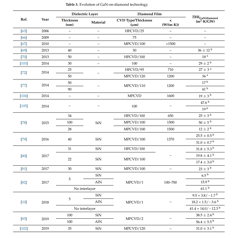
In 2019, HEMTs fabricated on latest generation Element Six GaN-on-diamond wafers(with a 30 nm-thick dielectric layer) showed 2.95 Kmm/W Rh, 56 W/mm DC power capability, and average/maximum channel temperature of 176/205 °C (101]. Nevertheless, these devices had high leakage currents which ultimately limited their break down voltage, showing there is still some room for optimizing the fabrication process and maximizing the performance of GaN-on-diamond HEMIs. In the same year, researchers from RFHIC (102] reported the fabrication of 4” GaN-on-diamond wafers with a TBRGaN/diamond of 31.0 m2.K/GW and an uniformity of ±10%. The development of an inner slot via hole process allowed the opening of 10 um-diameter holes in the diamond using a laser drilling process--Figure 5. On-wafer pulsed load-pull tests performed at 2 GHz revealed18.1 W/mm Pp for an encapsulated 10 x 200 um gate HEMT.

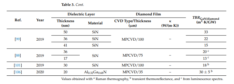
The evolution of the relevant technological parameters (dielectric material and thickness, diamond film k, and value of TBRGaN/diamond) since 2006 is listed in Table 3. It can be seen that most of the GaN-on-diamond HEMTs fabricated by this method feature a ~30 nm-thick SiN layer, and a TBRGaN/diamond in the range of 20-30 m2.K/GWSection 4.1 describes in more detail the impact of the dielectric layer on the experimental TBRGaN/diamond values and the electrical parameters of GaN-on-diamond HEMTs fabricated so far using this method are summarized in Table A1 in the Appendix A.


CSMH focuses on the research and production of diamond wafers, and currently has diamond wafer, diamond heat sink , GaN on diamond ,AIN on diamond and other products, providing diamond thermal management solutions for our customers.
 闽ICP备2021005558号-1
Leave A Message