Pos:
Home KnowledgeTechnologyHeat dissipation nova | diamond heat sink, thermal management of the new radiator for electronic device materialsElectronic devices and their applications are one of the fastest growing fields, with feature sizes leaping from the micron to the nano scale in just 20 years. As transistors decrease in size and density, computing power increases, but from the point of view of devices, chips and systems, power consumption inevitably increases. The power of the HPC module has reached 200-250W, and the thermal load of the processor in the four-slot computing system is close to 1 kW. High power dissipation inevitably affects electronic device systems and data centers, etc. Power density and its spatial distribution at the chip level are also noteworthy, and may have important effects on chip reliability and thermal management. With the development of nanoscale electronic devices and flexible electronics such as 3D chip structures, it is now more urgent than ever to solve thermal management problems.

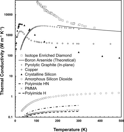
Figure 1. Temperature effect of thermal conductivity of bulk materials. (Isotopically purified diamond, gallium boride, pyrolytic graphite, copper, crystalline silicon, amorphous silicon dioxide, polymethyl methacrylate and polyimide)
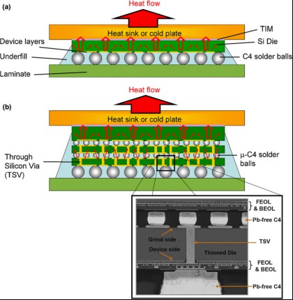
Transistor design improved and chip layers increased, (a higher density of interfaces and boundaries within the die structure, (A higher density of interfaces and boundaries within the die structure, each of which can act as a thermal impedance to heat flow). Each of which can act as a thermal impedance to heat flow.

Figure 2. Structure design of MOSFET
For electronics, overall reliability depends on the hottest area on the chip rather than the average temperature of the chip. Thus, hot spots often determine the required packaging and thermal management solutions, such as material selection, radiator and cold plate design, and pumping power required at the system and facility levels.

Figure 3. Chip package
CSMH is a high-tech enterprise focused on the development and production of third generation (wide gap) semiconductor substrate materials and devices, and is committed to becoming the world's leading wide gap semiconductor materials and devices company. We always uphold the concept of customer first, to provide customers with the best products and services. At present, the company has achieved large-scale production of diamond and aluminum nitride related products. The existing Diamond wafer Ra<1nm, the thermal conductivity of diamond heat sink 1000-2000W/m.k, and GaN on diamond, Diamond on GaN, diamond-based aluminum nitride and other products. And has been widely used in 5G base stations, lasers, new energy vehicles, new energy photovoltaic and other fields. Here, we will provide you with the most comprehensive device thermal management solutions.
 闽ICP备2021005558号-1
Leave A Message