Pos:
Home KnowledgeTechnologyBorn to reduce fever! The 6G era is coming, and CVD diamond wafer is ready for developmentFrom 1G to 5G, mobile communication technology has achieved a qualitative leap forward, bringing great convenience to human life and production. The 6G technology currently under development will build a fully connected world with the integration of terrestrial wireless and satellite communication. The transmission capacity may be 100 times higher than that of 5G, and the network delay may be reduced from milliseconds to microseconds. The peak rate, delay, traffic density, connection number density, mobility, spectrum efficiency, positioning capability and other aspects will be comprehensively optimized and upgraded. To further narrow the digital divide and achieve the "ultimate goal" of the Internet of everything.
6G is coming, heat dissipation demand is increasingly prominent
The 6G era is coming, which is bound to involve the upgrading of key devices, from the core chip to the RF device, to the base station end to the application end, all need to be transformed and upgraded. With people's increasing demand for the lightness and high performance of electronic products, the power density of semiconductor components continues to increase, and the heat flux will be larger and larger, some of which can even reach tens of kilowatts per square centimeter, 5 times that of the surface of the sun. How to heat and cool the material has become the primary problem.

So in the field of heat conduction and heat dissipation, how to choose the material?
At present, the popular cooling solutions mainly include graphite sheet, graphene, thermal interface material (TIM), heat pipe (HP) and soaking plate (VC), and semi-solid die casing. Natural graphite cooling film products are thick, and the thermal conductivity is not high, it is difficult to meet the future high power, high integrated density device heat dissipation requirements, but also does not meet people's requirements for ultra-thin, long endurance and other high performance. Therefore, it is of great significance to search for new superthermal conductivity materials.
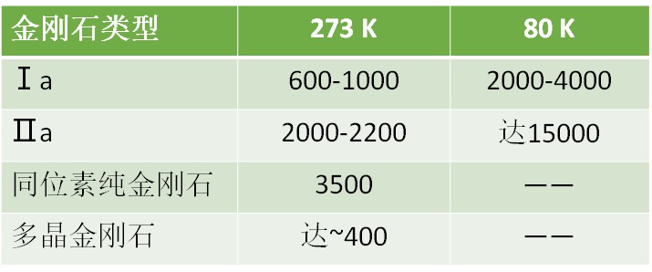
Diamond, as a representative of the above materials, has the highest thermal conductivity in nature. At room temperature, the thermal conductivity (Type Ⅱ Diamond) can reach 2000 W/(mK), the coefficient of thermal expansion is about (0.86±0.1)*10-5/K, and it is insulated at room temperature. In addition, diamond also has excellent mechanical, acoustic, optical, electrical and chemical properties, and has obvious advantages in the heat dissipation of high-power photoelectric devices. Therefore, diamond has great application potential in the field of heat dissipation.

Table: Thermal conductivity of diamond (Wm-1k-1)
Principle of diamond thermal conductivity
Diamond is a cubic crystal, formed by carbon atoms bonded together through covalent bonds. Many of diamond's extreme properties are the direct result of the strength of the sp³ covalent bond that forms the rigid structure and the action of a few carbon atoms. In contrast to metals, which conduct heat through free electrons and whose high thermal conductivity is associated with high conductivity, heat conduction in diamond is accomplished only by lattice vibrations (i.e. phonons). The extremely strong covalent bond between diamond atoms gives the rigid lattice a high vibration frequency, so the Debye characteristic temperature is as high as 2,220 K. Since most applications are much lower than Debye temperature, phonon scattering is small, so the heat conduction resistance of phonon medium is very small.
CVD diamond has very high thermal conductivity. At room temperature, the thermal conductivity of diamond is five times that of copper. At the same time, it itself is an excellent insulating material, so diamond film is the best choice for the production of high power photoelectronic components radiator material in the 6G era. The future is coming, heat dissipation diamond will help 6G technology fly.
CSMH is a high-tech enterprise focusing on the development and production of third generation (wide gap) semiconductor substrate materials and devices, and is committed to becoming the world's leading wide gap semiconductor materials and devices company to provide the most beautiful thermal management solutions. The existing core products are diamond wafer (Ra < 1nm), CVD diamond heat sink (thermal conductivity up to 1000-2000W/m.k), diamond-based gallium nitride epitaxial sheet, diamond-based aluminum nitride film, etc., which can be used in the production of high power optoelectronic components. At present, high-power semiconductor lasers using diamond heat sink have been used in optical communication, RF power amplifier, laser diode, power transistor, electronic packaging materials and other fields are also used.
 闽ICP备2021005558号-1
Leave A Message