Pos:
Home KnowledgeTechnologyOptical and thermal properties of CVD diamond wafer for integration with power electronicsDevice self-heating is a principal limiting factor in high-power electronics. Better thermal management, e.g., through diamond heat spreading layers, is necessary for increasing power densities and efficiencies while reducing device size and mitigating device failure . Diamond grown by chemical vapor deposition (CVD) produces thin films of good quality, but the first ∼100 nm, called the coalescence layer, is generally characterized by smaller grain size and concomitantly higher grain boundary density. The latter often implies a higher non-diamond carbon content . This layer is known to hinder heat flow from the device active region into the diamond , a process which is impeded even for ideal hetero-interfaces . The polycrystalline grain structure and columnar texture of CVD diamond films also result in substantially lower in-plane thermal conductivity (κ) when compared to bulk crystals . To understand and improve thermal management of devices incorporating polycrystalline diamond films as heat spreaders, it is necessary to reliably characterize their thermal properties.
Studies of diamond material for thermal management are reported for a nominally 1-µm thick layer grown on silicon. Thickness of the diamond is measured using spectroscopic ellipsometry. Spectra are consistently modeled using a diamond layer taking into account surface roughness and requiring an interlayer of nominally silicon carbide. The presence of the interlayer is confirmed by transmission electron microscopy. Thermal conductivity is determined based on a heater which is microfabricated followed by back etching to produce a supported diamond membrane. Micro-Raman mapping of the diamond phonon is used to estimate temperature rise under known drive conditions of the resistive heater. Consistent values are obtained for thermal conductivity based on straightforward analytical calculation using phonon shift to estimate temperature and finite element simulations which take both temperature rise and thermal stress into account.

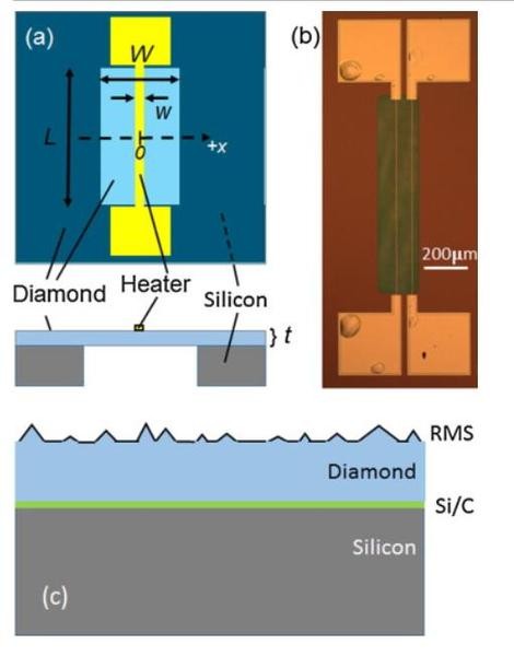
Fig. 1. A schematic (a) and optical image (b) of the diamond membrane, and (c) depicts the model used to fit the spectroscopic ellipsometry data.
Thermal conductivity for thin diamond films grown on silicon substrates have been measured using micro-fabricated test structures. Resistive heaters are formed on nanocrystalline diamond films grown on a substrate followed by back-etching of the silicon in an area directly below the heater to produce a diamond membrane . The design is depicted in Fig. 1(a). Heat initially flows from the resistor and remains restricted to the diamond before eventually flowing into the substrate.
Because the linear thermal expansion of diamond and silicon differ, residual stress on a uniform CVD diamond film will occur following growth and cooling to room temperature. This thermal stress is compressive when diamond is grown at temperatures under 1220 °C, as is the case here. Because the membranes are small in lateral dimension, the overall stress is expected to change little upon membrane formation. This is confirmed by our micro-Raman measurements. During calibration, the increasing temperature will produce thermal stress in the tensile direction due to expansion of the thick silicon substrate. The measured dependence agrees with this expectation. In contrast, when driving the micro-fabricated heater, the silicon temperature rise is negligible so that primarily the membrane will expand. Therefore, under drive conditions the membrane thermal stress will be in the compressive direction.

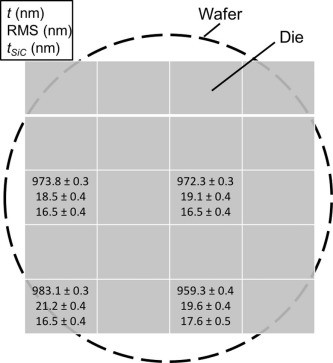
Fig. 2. Die locations of a diamond/Si wafer where SE measurements are done. Non-uniformity in the diamond thickness is less than 1%.
Fig. 2 shows the results of measurements at different die locations from the wafer. Each measurement was carried out post-heater fabrication, back etching, and dicing. Good consistency is obtained for all model parameters examined: diamond thickness, RMS roughness, and Si/C thickness. Measurements from several positions on given die likewise produced good agreement. The diamond thickness values obtained a range from 959.3 to 983.1 nm with mean value 972.1 nm, in good agreement with the nominal 1-μm from the CVD growth. Measurements taken on the same die (not shown) were likewise consistent. Spot checks of thickness and roughness from electron microscopy cross-sections are in good agreement, with the RMS roughness estimated at ∼18 nm. Our results show desired cross-wafer uniformity is obtained from the growth.

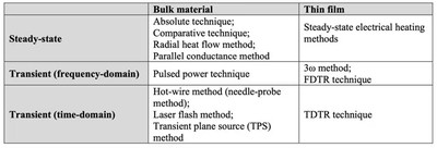
For the detection of diamond wafers, CSMH adopts the scientific and accurate TDTR method. TDTR detection, that is, the cross-sectional thermal conductivity of diamond samples was measured with a time domain thermal reflectometry (TDTR) system. TDTR is a relatively accurate optical pump-probe method that can be used to characterize the thermal transport properties of various forms of materials, including bulk, thin films and even liquids. The thermal conductivity of diamond wafer and diamond heat sinks of CSMH has been tested to reach 1000-2000W/m.k, and the test results may be slightly different due to different testing instruments.
 闽ICP备2021005558号-1
Leave A Message