Pos:
Home KnowledgeTechnologyContactless Thermal Boundary Resistance Measurement of GaN-on-Diamond WafersAlGaN/GaN high electron mobility transistors (HEMTs) have greatly contributed to the high-power RF amplifier field. However, managing waste heat is an increasingly important consideration when extending GaN RF HEMT operation to ultra-high-power densities. Low thermal resistance GaN-on-diamond wafers offer enhanced thermal management with respect to GaN-on-SiC devices. The GaN/diamond interfacial thermal resistance can contribute significantly to the total device thermal resistance and must therefore be minimized to gain the maximum benefit from GaN-on-diamond. A contactless thermoreflectance measurement technique has been developed, which can be used after wafer growth and before device fabrication, enabling rapid feedback about the influence of growth parameters on interfacial thermal resistance.

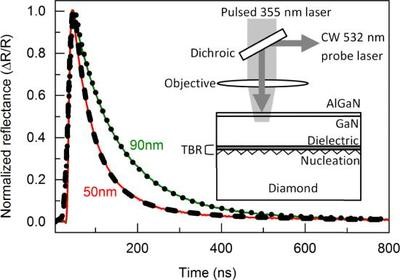
Fig. 1.Thermoreflectance signal measured on two GaN-on-diamond wafers with 90 nm and 50 nm-thick dielectric layers.
Fig. 1 shows the thermoreflectance signal measured for the GaN-on-diamond wafers at an ambient temperature of 25 °C, normalized to the peak reflectivity modulation. Only a few seconds is needed to record each trace, enabling fast wafer mapping. On each sample, repeat measurements at five locations produced indistinguishable results. A clear decrease in the thermal relaxation time constant is observed for the sample with a 50 nm-thick dielectric layer with respect to the sample with a 90 nm-thick layer, indicating a reduction in thermal resistance.

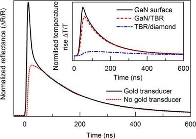
Fig. 2.AS INSET: Modeled transient temperature rise at the GaN surface, GaN/TBR interface and TBR/diamond interface, using a GaN/diamond TBReff=4.0×10⁻⁸ m2 K/W.
The inset of Fig. 2 shows the modeled temperature transient, for illustration assuming a TBReff value of 4×10⁻⁸ m2 K/W. The vertical temperature gradient generated across the GaN layer relaxes after 75 ns and only a small temperature difference (Δ T) is observed across the diamond substrate. After 75 ns the remaining Δ T is predominantly across the TBReff layer only. Consequently, the TBReff value is the only sensitive parameter in fitting the temperature decay in the >100 ns region; This was verified by adjusting the GaN and diamond thermal conductivity by ±25%, which had no discernable effect on the simulated temperature transient during this timescale. The observed ∼2× reduction in TBReff with decreasing dielectric layer thickness highlights that this layer is responsible for a significant proportion of the total interface thermal resistance and that its thickness should be reduced as far as possible. The limiting factor for reducing the dielectric layer thickness is the requirement that the correct conditions for diamond nucleation and growth are maintained at this interface.

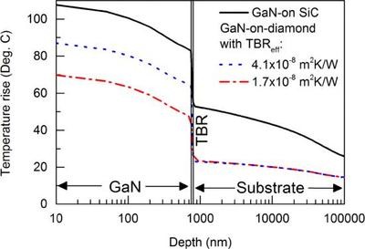
Fig. 3.Thermal simulation of the vertical temperature profile beneath the central finger of an 8 finger AlGaN/GaN-on-diamond HEMT at a power dissipation of 5W/mm.
Fig. 3 illustrates the simulated vertical temperature profile beneath the central gate finger; A GaN-on-SiC device with the same geometry is shown for comparison, assuming κSiC=450 W/mK and a representative TBReff value of 2×10⁻⁸ m2 K/W . Based on the modeled temperature rises, power dissipation can be increased by 25% for the GaN-on-diamond wafer with the 50 nm dielectric (TBReff=1.7×10⁻⁸ m2 K/W), with respect to the thicker 90 nm dielectric layer (TBReff=4,1×10⁻⁸ m2 K/W), highlighting the benefit of growth optimization based on measurement results. At the same channel temperature rise, power dissipation can be increased by 50% for the GaN-on-diamond wafer with improved TBReff with respect to GaN-on-SiC. An even further reduction in GaN-on-diamond thermal resistance is anticipated by reducing the dielectric layer thickness further. Combined with gate pitches optimized specifically for GaN-on-diamond, total output power >3× greater than GaN-on-SiC will be achievable.
A measured 2× reduction in the GaN/diamond interfacial resistance is achieved by reducing the dielectric thickness between the GaN and diamond from 90 to 50 nm, enabling a potential 25% increase in transistor power dissipation for GaN-on-diamond.A rapid contactless interfacial thermal resistance measurement technique has been demonstrated for GaN-on-diamond wafers. This technique can be applied after wafer growth, enabling mapping and screening of interfacial thermal resistance before device fabrication. Furthermore, TBReff values can be reduced by to tuning growth parameters, with an associated improvement in transistor thermal resistance.
CSMH has been conducting GaN&Diamond research for more than ten years, and has achieved breakthroughs in all three GaN&Diamond combination schemes. Existing diamond heat sinks for GaN on Diamond, Diamond on GaN and GaN&Diamond bonding, benchmarking against world-class standards. CSMH's existing diamond heat sink and diamond wafer product technical indicators have reached the world's leading level. The surface roughness of the diamond wafer growth surface is Ra<1nm, and the thermal conductivity of the diamond heat sink is 1000-2000W/m.K. We will continue to innovate in science and technology, strive to be the driver and contributor of technological progress, and let cutting-edge technologies help relevant application fields take off.
 闽ICP备2021005558号-1
Leave A Message