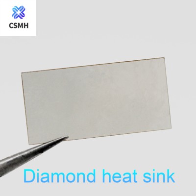
Industrial diamond is considered the supreme semiconductor for cutting losses during power transmission over long distances. While silicon is today the star of semiconductors, diamond could replace it in the following decades. With superior electronic and thermal capacities, this replacement provides many possibilities in power transmission, bionics, or aeronautics, if its cost drops.
Replacing silicon-based semiconductors of a converter, with a diamond, it is to cut energy losses in power transmission from offshore wind farms. For power electronic applications, one of the most important factors is the breakdown field of the material. In the case of silicon, it is equivalent to 300,000 V/cm, which is quite low. In the case of diamond however, the breakdown field is 10 MV/cm.
To withstand a voltage of 1,000 V, a converter would require a layer of 100 microns, which leads to a significant resistance, compared to 1 micron for diamond. With this change, it is estimated that energy losses can be reduced by four-fold.
Electromobility
At an equivalent power, but with a reduced size, diamond provides new paths for applications in bionics and transport. The weight of the material being the number 1 enemy in vehicle design, this replacement becomes very interesting.
If weight reduction is involved in smaller volumes of materials, high temperature resistance is also a major argument in these applications. Beyond 150°C, silicon’s properties change and are no longer optimal. Diamond can easily rise to 300°C. As a result, where a silicon converter requires a complex cooling system, diamond offers simpler and easier solutions. “In the case of aircraft electrification, we can imagine the transition from a 400 kg to 50 kg converter, which would be a huge gain,” an expert explains.
Essential features of diamond as an advanced semiconductor material
· Diamond is a better heat dissipation than metals. Its thermal conductivity is around 2200 W/mK or 5 times copper conductivity.
· Diamond is made of carbon. Each carbon atom is in a rigid tetrahedral network, where it is equidistant from neighbouring carbon atoms, giving it much of its superlative properties.
· Diamond can be made in the laboratory. Two techniques are used to synthesize it: HPHT (High Pressure High Temperature) or MPCVD (Microwave Plasma Chemical Vapor Deposition).
· Diamond can be doped to become more or less conductive. Diamond can be of type p, doped with boron (B), or of type n, doped with nitrogen (N) or phosphorus (P).
· Implantation doping is not effective in diamonds. That is why in situ doping is done: doping species are incorporated during the process.
· Diamond is also a superconductor at low temperatures (-269°C).
· Diamond is a very wide band gap material. Its band gap is 5.5 eV, five times greater than the silicon one at 1.1 eV. The wider the band gap, the lower the influence of temperature on intrinsic carrier concentrations. This property led it to be classified as an insulator until doping was successful.
· Diamond's breakdown field is 30 times greater than silicon’s, which allows diamond’s diodes and transistors to withstand voltages of thousands of volts in the off state.
· More current due to fast charging. The electrons in diamond have great mobility, which allows to reduce the joule effect losses while the diamond's diodes and transistors are in on state.
· With a Young modulus of 1000 GPa the diamond is by far the hardest semiconductor.
CSMH, a wide bandgap Semiconductor Material and Device company manufacturing with unique technology.
Products including: high quality diamond wafer, diamond heat sink, GaN & Diamond wafer and AlN on various substrate like Si,Sapphire and Diamond etc. Our product's performance has improved to a level that is among the best in the world after more than 10 years of technological development. The company has built an intelligent manufacturing plant, started mass production of diamond wafers, and has a substantial intellectual property (IP) portfolio.
For more info.: globalsales@csmh-semi.com

 闽ICP备2021005558号-1
Leave A Message