Pos:
Home KnowledgeTechnologyKing of Heat Dissipation - What are the application fields of diamond wafers?hanks to its excellent intrinsic properties, diamond is promising for applications of high-power electronic devices, ultraviolet detectors, biosensors, high-temperature tolerant gas sensors, etc.
Due to limitation of its bandgap energy, thermal conductivity, and electron saturation velocity, Si-based electronic devices cannot meet future demands in fields of high-power, high-temperature, high-frequency, and low power loss. Wide bandgap semiconductors such as SiC, GaN, and diamond are developed to partly replace Si for next-generation power electronic devices. Compared with other semiconductors, diamond has the widest bandgap energy, the highest breakdown field, the largest thermal conductivity, and the largest carrier mobility. Therefore, diamond-based electronic devices are promising for future applications in the fields of high-power handling, high-temperature operation, and high-frequency switching. Meanwhile, since diamond has good chemical inertness, good biocompatibility, and a large electrochemical window, it is also a suitable candidate for applications of biosensors. Additionally, diamond can also be applied in fields of ultraviolet (UV) light-emitting diodes, UV detectors, and high-temperature tolerant gas sensors.
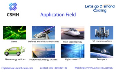
CSMH is the first company in China to master the core process of MPCVD to prepare high-quality diamond wafer and started mass production, and it is the first in the world to create an efficient and precise machining method for diamond atomic-level surface based on plasma-assisted polishing. The surface roughness of the diamond heat sink is reduced from tens of microns to below 1 nm, reaching the semiconductor-level application standard. Based on wafer-level diamond product capabilities, the company has developed GaN-on-diamond epitaxial wafers, which are mainly used in radio frequency (satellite, 5G base station) and high-power devices (photovoltaic, wind power, new energy vehicles, energy storage) and other areas with high thermal management requirement, as a complement to GaN-on-SiC materials.
The company will invest heavily in R&D and innovation, continue to break through technical difficulties, and make continuous efforts to solve the bottleneck problem of heat accumulation in high-power density devices in the future.

 闽ICP备2021005558号-1
Leave A Message