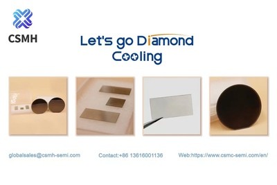
Thin and thick film resistors are common components in electronic circuits. Typically RF resistors are made of thin lossy strips of metal – TaN (Tantalum nitride) or NiCr (Nickel chromium) – on dielectric substrates. The increasing parasitic (stray) inductive and capacitive losses at higher frequencies result in increasing signal distortions. With the decreasing value of inductance at GHz frequencies, extra attention is paid to minimizing the capacitance between the thin film and ground-plane. The lower dielectric constant of diamond compared to other common resistive substrates (BeO and AlN) allows the use of thinner substrate for a given resistor area, with as much as 4-6 times higher thermal conductivity.
As an example for 50 Ω resistor dissipating 100 W and not exceeding 125°C at 1.25 VSWR, the use of a diamond substrate enables operation at frequencies above 12 GHz. A BeO or AlN substrate would limit operating frequencies to below to 4.2 and 2.9 GHz respectively.
Key to succesful implementation of CVD diamond for high frequency applications.
In order to achieve full heat-spreading or resistive effectiveness of diamond in the overall system design, package integration issues as well as functional requirements need to be carefully considered and optimized.
Surface Preparation – The surfaces of electronic components are typically very flat and smooth. The successful implementation of CVD diamond heat spreader is dependent on matching the same level of flatness and smoothness onto the spreader. It is possible to achieve surface roughness of the order of 15 nm Diamond Thickness – The thickness of the CVD diamond is directly proportional to the ability to spread heat and increasing total thermal resistance. For a range of applications and particularly for devices with high power density over very small areas, thickness in the range of 250 to 400 microns is sufficient. The isotropic thermal characteristics of CVD diamond facilitate spreading of the heat efficiently and hence reduce maximum operation temperature at a constant power output. However, when cooling disk lasers with optical output power of several kW, the use of diamond heat spreaders of the order of several millimeters in thickness has proven to be crucial for successful operation. Functional Considerations – In using CVD diamond for thermal applications, there are some functional requirements that are dependent on the application. One is the electrical conductivity of the heat spreader itself. For a range of devices, it is easiest to run the drive current through the device and the heat spreader for ground contact. This is a typical configuration for example in laser diodes. For other devices, the heat spreader itself is required to be insulating by keeping the side faces free of metallization. Summary Significant thermal-management improvements to electronic systems can be realized by using CVD diamond. The integration can be relatively straightforward as the CVD diamond can be a direct replacement to AlN (Aluminium nitride), BeO (Beryllium oxide) or other advanced ceramics. Attention to detail at the interfaces is important to keep overall thermal resistance low and thereby optimizing the effectiveness of the diamond. Through improved synthesis technology, advance processing and on-going cost reduction efforts, CVD diamond has become a crucial enabler as a heat spreader and heat dissipater for high power density RF applications. It is expected, that this trend will continue in the years to come, in line with the ever increasing need for smaller and more powerful electronic devices and systems. An additional factor will be the rapidly increasing RF frequency in defense-related as well as upcoming 5G wireless applications. CSMH, located in Xiamen, is partners with Fujian Province Semiconductor Manufacturing Cluster, the Semiconductor Research Institute of Ajou University and Jimei University. The technical indicators of the existing diamond heat sinks and diamond wafer products of CSMH have reached the world's leading level. The surface roughness of the diamond wafer growth surface is Ra<1nm, and the thermal conductivity of the diamond heat sinks reaches 1000-2000W/m. The company has built an intelligent manufacturing plant, started mass production of diamond wafers, and has a substantial intellectual property (IP) portfolio. In the near future, the CSMH will keep expanding its international sales and service network, as well as its development of global customer resources, in an effort to be the global leading provider for wide-bandgap semiconductor devices and materials.
 闽ICP备2021005558号-1
Leave A Message