Pos:
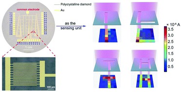
Home KnowledgeTechnologyPolycrystalline Diamond Wafer Photodetector Planar Arrays For Solar-Blind ImagingIt was shown that a wafer-sized high-quality polycrystalline diamond is prepared using microwave plasma chemical vapor deposition. Solar-blind photodetector arrays with 6 × 6 cells are demonstrated with the polycrystalline diamond. The photodetector array shows good uniformity and stability, a responsivity of 255 mA W−1 at a wavelength of 218 nm and at a bias of 30 V, and a relatively fast response speed (1.2 ms/0.51 ms). Using the planar photodetector array as the sensor unit of an imaging system, clear images can be obtained. This is the first report for photodetector planar arrays based on polycrystalline diamond. Our results indicate that polycrystalline diamond may be used to develop large-area optoelectronic devices.

The thermal conductivity of diamond is one of its most remarkable properties. It exceeds by several folds the thermal conductivity of all other solid materials: metals, semiconductors and dielectrics, including copper, which is used most frequently to remove heat in electronics. Diamond is also applied as a highly effective heat sink material in other semiconductor devices, such as avalanche and Gunn diodes.
CSMH can supply high quality diamond wafers as effective heat sink bases for semiconductor devices. With more than 10 years of technological development, CSMH has made breakthroughs. We currently produce diamond wafer, diamond heat sinks with the thermal conductivity reaches 1000-2000W/m.K. Our products were designed for "heat dissipation," and are widely utilized in the applications of high-power, high-frequency, and high-temperature electronic devices.
 闽ICP备2021005558号-1
Leave A Message