Pos:
Home KnowledgeTechnologyDiamond wafer: Low loss optical structure for directional and efficient photonThe development of nanoscale optical antennas with efficient single photon sources has been widely explored for various quantum optics devices. Single photon emitter-based optical antennas are crucial to quantum sensing and quantum computation devices due to their precise control over qubit generation. Different kinds of single photon emitters such as quantum dots, single molecules, 2D materials, defects in solid state systems have already been comprehensively studied. The main problem with all of these systems is insufficient photon emission and short lifespans. NV centers in diamond, however, show a better emission profile and spin coherence time at room temperature, which makes them suitable for measuring optical readout fidelity in magnetometry and quantum information devices. The similar optical transistor and intensity router applications in diamond nitrogen-vacancy center, phase transition and crystal-field splitting of solid atomic-like media quantum device are studied theoretically and experimentally. One major limitation of NV center is that only a very small number of emitted photons can be
collected via conventional procedures, which limits the sensitivity of NV center based devices. The high refractive index contrast between diamond (~2.4) and air causes the maximum number of outgoing photons to reflect through total internal reflection on diamond substrate. As a result, collection efficiency significantly decreases. Different nanostructures have been adopted to overcome this problem and improve the efficiency of detecting photons towards the collection aperture. A few structures, such as solid immersion lens (SIL) based structures and diamond nanopillars, play a crucial role for specific applications.
Furthermore, during the experimental fabrication process, the optical structure should be cost-effective and relatively simple to make in order to be compatible with commercial technology.
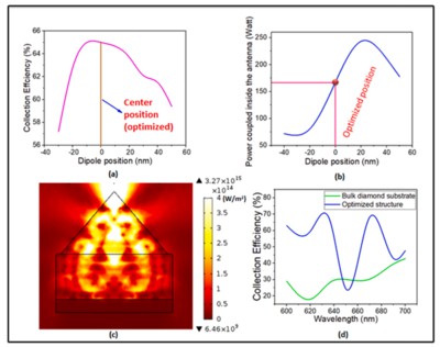
A simple diamond nanostructure based on a rectangular and pyramidal geometry is presented here. We numerically investigate the collection efficiency and the losses caused by coupling power inside the device. In this system, device parameters have been optimized for optimal waveguide performance. This optical structure generates a highly directional far field output beam as well as enhancement in collection efficiency near zero phonon line (ZPL) of NV center in diamond. Whereas other antennas perform well within the regime of NV emission spectra, our optimized structure ensures better enhancement in collection efficiency compared to ordinary diamond substrate exactly near the ZPL emission (at 637 nm). In addition, the geometric tolerances have been taken into consideration to allow for the error flexibility in the experimental fabrication of the device. Our design concept can be fabricated with the focused ion beam (FIB) technique, which allows us to design high-sensitivity nano-range optical structures for quantum sensing and processing applications.

CSMH focuses on the R&D and production of diamond wafers, and has created an efficient and precise machining method for diamond atomic-level surfaces based on plasma-assisted polishing, diamond wafer Ra<1nm, diamond heat sink thermal conductivity 1000-2000W/m.k, and GaN on diamond, Diamond on GaN, diamond-based aluminum nitride and other products. We will keep pursuing the innovation-driven development strategy in the future, offering our customers products of high quality and reliable performance while contributing the rapid development of the global semiconductor industry.
 闽ICP备2021005558号-1
Leave A Message