Pos:
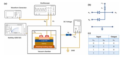
Home KnowledgeTechnologyDiamond Wafer Application in Schottky diodes fabricated by selective growth methodThe drastic miniaturization of high-frequency electronic devices has led to a dramatic increase in the local operating temperatures of individual components. Diamond microprocessors and logic chips are expected to operate under high-temperature and high-radiation environments. A logic gate circuit, based primarily on the use of diodes, constitutes the building block in the fabrication process of these chips. Diamond Schottky diodes were fabricated by a selective growth method using a noble metal (Ti/Ru) mask. The rectification ratio of the Schottky device was as high as 7x10⁹ at 633 K, indicating good high-temperature performance. Various methods have been used to extract the parameters of Schottky diodes, and the applicability of these methods has been compared. Astable logic AND gate circuit, operating at 633 K, was achieved using these Schottky diodes, implying their great potential for implementation in chips working under high-temperature conditions.
Diamond has a wide band gap, high thermal conductivity, high carrier mobility, high breakdown field, high carrier saturation velocity, and high displacement energy. The combination of these properties makes diamond an excellent candidate material for a broad range of applications encompassing high-temperature, high-voltage, high-frequency, and high-radiation environments. Many electronic devices have been developed for various applications, including MOSFETs, heat sinks, detectors, nuclear batteries, and electrochemical, applications.Gallium nitride (GaN)-based microprocessors have been proposed for space applications owing to their high-temperature operation. Nevertheless, diamond outperforms silicon (Si) and GaN in terms of bandgap, carrier mobility, and displacement energy, thereby making it more suitable for use in high-temperature and high-radiation environments. Therefore, future technologies should consider diamond replacing silicon in microprocessors used for deep-space exploration and nuclear power plants.

CSMH focuses on the R&D and production of diamond wafers, and has created an efficient and precise machining method for diamond atomic-level surfaces based on plasma-assisted polishing, diamond wafer Ra<1nm, diamond heat sink thermal conductivity 1000-2000W/m.k, and GaN on the diamond, Diamond on GaN, diamond-based AlN and other products. We will keep pursuing the innovation-driven development strategy in the future, offering our customers products of high quality and reliable performance while contributing to the rapid development of the global semiconductor industry.
 闽ICP备2021005558号-1
Leave A Message