Pos:
Home KnowledgeTechnologyLoved by electronic engineers, diamond wafer is the best choice for heat dissipation!At present, the miniaturization of electronic devices and integrated thermal management present new challenges for electronic engineers. Hot spots have become a key thermal feature of today's high-power density electronics, such as central processing units, laser dioxides, and insulated gate bipolar transistors, where hot spots can have a heat flux of 1000 W/cm² or more. At such a high heat flux, insufficient heat dissipation can lead to an excessively high temperature increase, which can reduce equipment performance and accelerate equipment failure. Therefore, for high-density electronic devices, heat dissipation is the main research direction.At present, the miniaturization of electronic devices and integrated thermal management present new challenges for electronic engineers. Hot spots have become a key thermal feature of today's high-power density electronics, such as central processing units, laser dioxides, and insulated gate bipolar transistors, where hot spots can have a heat flux of 1000 W/cm² or more. At such a high heat flux, insufficient heat dissipation can lead to an excessively high temperature increase, which can reduce equipment performance and accelerate equipment failure. Therefore, for high-density electronic devices, heat dissipation is the main research direction.
As the hardest substance in the world, diamond has excellent properties in electronics and electrical that cannot be achieved by other semiconductor materials, including:
1. Extremely high operating temperature: The working temperature exceeds 300°C (5 times higher than silicon), which solves the problem of cooling in some applications.
2. Extremely high thermal conductivity: The highest thermal conductivity of any known material. If needed, it dissipates heat, is 90% more efficient and reduces energy loss by 90% compared to silicon.
3. High dielectric strength; More than several orders of magnitude of silicon (seventh power of diamond 1x10, fifth power of silicon 3x10).
4. Low dielectric constant: low dielectric constant in microelectronic circuits and reduce crosstalk. Diamond: 5.5 to 5.7; Silicon: 11.8 to 11.9; Silica (3.5).
5. Radiation resistance: Due to the extremely short carrier life (about 2 microseconds), the radiation resistance is excellent.
6. High hardness and high strength; Suitable for MEMS devices.
7. Ultra-wide optical transparency, from ultraviolet to infrared.
8. Very low coefficient of thermal expansion: A low coefficient of thermal expansion (CTE) is equal to reducing the stress at the thermal interface.
9. Very wide band gap: Egap = 5.47 eV.
10. High flowability: 4500 cm2/(V.S) is used for electrons in single crystal CVD diamond, with excellent performance for high frequency operation and FETs above 50 GHz.

Figure 1 Comparison of the characteristics of diamond and some semiconductor materials
Diamond is converted from one of the best electronic insulating devices into highly conductive pseudometals, eventually forming a superconductor by adding impurities or dopants. Features such as optical colors are also altered by doping or impurities. Diamonds are doped with boron (B), forming p-type diamonds and phosphorus in the n-type region. Nitrogen (N) is doped to produce n-type semiconductors, but they may be more suitable for biosensors, magnetic field strength meters, quantum optics, and spintronics devices. Theoretically, diamond semiconductor devices can drive circuits to frequencies up to 400 GHz, and diamond-based semiconductors are ready to make progress on complex devices such as high-speed and high-power FET transistors. RF and microwave electronics, high-power switching, MEMS and high-efficiency passive devices. These faster, thinner, and cooler diamond devices will lead to more powerful supercomputers, advanced radar and telecommunications, efficient hybrid vehicles, a comprehensive electronics environment, and next-generation avionics instruments. Diamond MEMS devices can be said to be specially designed for capacitive switch arrays, providing better dynamic tuning antennas for high-end smartphones. Diamond technology may even extend Moore's Law beyond its intended demise.

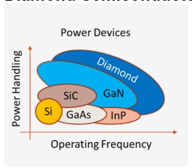
Figure 2 Frequency semiconductor materials of different groups of power supply processing and operation
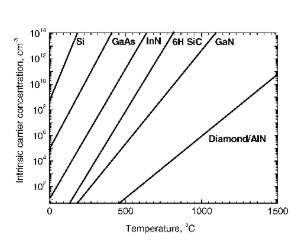
Diamond and other compound semiconductors, such as silicon carbide, gallium carbide, gallium arsenide (GaAs), and gallium nitride (GaN) as a wide bandgap (WBG) semiconductor, exhibit superior performance in their fields. Power handling at high operating frequencies is superior to conventional compound semiconductors such as SiC, GaAs, and gallium nitride compared to silicon. Traditional silicon and gallium arsenide devices do not apply to semiconductors due to their packaging, interconnection, inability to operate above 300°C, and thermal increases in carrier concentrations. Diamond semiconductor devices, on the other hand, should be immune to the effects of thermogenesis carriers, making them ideal carriers for high temperature and high voltage applications such as (power electronics (e.g., PIN diodes, junction effect transistors [JFETs] and thyristors)) or control in electronic thermal engines. High-voltage PIN diodes with high-temperature and high-frequency capabilities can manufacture high-performance, high-voltage power switches, power rectifiers, attenuators, photodetectors, and RF switches.

Figure 3 Variation of the intrinsic carrier concentration of several semiconductor materials by elevating the temperature
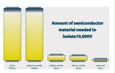
Diamond is known as the ultimate wide-bandgap semiconductor material thanks to its inherent properties: the thermal conductivity is 5 times that of copper and 22 times that of silicon, and diamond is not only an excellent thermal conductor, but also a good insulator. With current technology, the high dielectric strength of diamond can separate a thin layer of diamond from a huge voltage, and at an isolation voltage of 10,000V, the volume of diamond required is 50 times less than that of silicon. Smaller device sizes allow faster switching, and CVD diamond has a lower dielectric constant than other WBG semiconductors, which can better reduce the interference in series in integrated circuits. Alfred Grill conducted an experiment in IBM's research laboratory: a diamond-like (DLC) film modified with a dielectric constant of N fluorine (F) or silicon (Si), resulting in the synthesis of a diamond-like (DLC) film with a dielectric constant of 2.5, and inferred that the electrical and optical properties of the diamond-like film and the dielectric diamond film with a closed internal porosity would have even a lower dielectric constant.

Figure 4 Comparison of electrical insulation or insulation of the effectiveness of various semiconductor materials
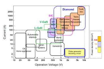
In the field of power electronics, diamond materials are likely to have the greatest impact. Photonics and high-power RF devices will also be transformed by the platform of diamond materials. As industrialization spreads technology, according to the International Energy Agency (IEA), World Electric expects energy production to grow by more than 75 percent, well above production in the last 20 years. Power electronics is the key to converting electrical energy from coal, fuel, gas or renewable primary energy sources, households, offices and plants. Fifty percent of the world's electricity is converted or controlled by silicon-based power supplies to electronic devices. These power converters are a major contributor to energy losses of about 80%. Along the power distribution system from primary power generation to the end user. The electronic properties of wide-bandgap diamond semiconductor materials can overcome the limitations of low-loss, high-efficiency energy conversion devices for silicon production.

Figure 5 Plot of potential operating voltage and current range for various power electronic materials platforms
CSMH focuses on the research and development and production of diamond, has the ability to design MPCVD equipment, is the first in China to master the core mass production of MPCVD to prepare high-quality diamonds, and creates an efficient precision processing method for the atomic surface of diamond based on plasma-assisted polishing, diamond wafer Ra < 1nm, diamond hot sink thermal conductivity of 1000-2000W/m.k, and GaN on diamond, Diamond on GaN, diamond-based aluminum nitride and other products, providing you with the most complete diamond thermal management solutions. At present, high-power semiconductor lasers using diamond heat sinks have been used in optical communications, and have also been used in RF power amplifiers, laser diodes, power transistors, electronic packaging materials and other fields.
 闽ICP备2021005558号-1
Leave A Message