Gallium nitride(GaN) is a wide bandgap compound llI-V semiconductor with highbreakdown electric field,high electron mobility, and high electron saturation velocity that translate in a tremendous potential for high power and high frequency applications(Table 1).The GaN high electron mobility transistor (HEMT)is a device that takes advantageof the two-dimensional electron gas (2DEG) that spontaneously forms at an aluminumgallium nitride (AlGaN)/GaN heterojunction thanks to the strong internal piezoelectricand spontaneous polarization. This 2DEG typically exhibits high values of sheet carrierdensity (1013 cm-2) and carrier mobility (1000-2000 cm2/(V·s)).
GaN HEMTs can be used in power switching for information technologies, automotive,healthcare, and industrial manufacturing applications. Thanks to the large bandgap,leakage currents in GaN power devices are orders of magnitude smaller than in silicon (Si),allowing for operation at higher temperature without thermal runaway and reducing thecooling requirements.The high breakdown electric field allows shorter drift distances for agiven blocking voltage, when compared to Si devices, yielding to a drastic reduction in the specific on-resistance that in turn translates into smaller device area and correspondingly lower capacitance. This reduces switching losses and enables higher switching frequencies.GaN HEMTS have also paved their way into mobile and satellite communications and radar systems. In addition to the properties listed above, the high breakdown electricfield of GaN allows higher matching impedances and circuits with broader bandwidth andhigh power-added efficiency(PAE).The ability of GaN to withstand higher temperaturesfurther increases the power density of a given HEMT device and power amplifiers withabsolute power levels of tens to hundreds of Watts have been reported.

Table 1.Selected properties of relevant semiconductors
Despite the fact that commercial HEMT devices based on a different combination ofprocesses and design technologies are currently available from a broad range of manu-facturers, GaN-based technologies still face some challenges that affect their overallperformance and limit their potential benefits.
1.Due to the intrinsic nature of the 2DEG,GaN HEMTs are normally-on (depletion mode) devices. For power switching applications, normally-off devices are preferreddue to static power consumption, simplification of circuit design, and safety concerns.Normally-off transistors can be obtained with different techniques, however theirperformance is typically worse than that of their normally-on counterparts.
2.The existence of electrically active surface traps located at the passivation/top-layer
interfaceand of bulk traps present in the GaN and buffer layers induceseffects such as current collapse, dynamic on-resistance (or knee walkout),degradation of cut-off frequency, and DC-RF dispersion, which compromisethe reliability of the devices and prevent harnessing the full potential of GaN HEMTpower devices.
3. Due to the intrinsic nature of GaN HEMTs, harsh and localized self-heating in the conducting channel may occur; this effect increases with the device power density and further compromises reliability.On one side, the electrical behavior ofthe traps mentioned in the above paragraph is temperature-dependent .On theother side, additional phonon scattering in the channel degrades the 2DEG effective carrier mobility, leading to degraded DC and RF performance. Finally, sincethe relation between the mean time-to-failure (MTTF) of an electronic componentand its operating temperature is semi-exponential, even a small temperature reduction can have a great impact on the lifetime of HEMTs with thermally-activated degradation mechanisms.
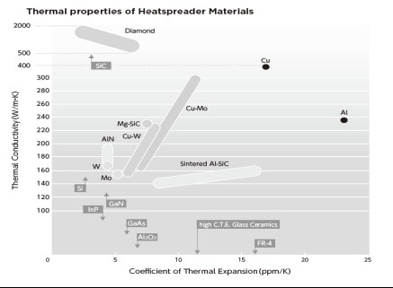
From what was described above, it can be concluded that the capability of efficientlytransferring the heat away from the localized hotspots and the consequent control of thedevice temperature is fundamental to achieve high levels of stability and reliability inHEMT applications [31]. Diamond has the highest thermal conductivity (K) of any bulkmaterial, and the integration of diamond films and GaN HEMTs as substrates or packaginghas already proven to enhance the extraction of the heat generated during the devicesoperation, leading to a substantial decrease in the junction temperature as well as to anincrease in the maximum power density the HEMTs can safely handle.This anticipates asuperior high-frequency handling capacity, higher energy efficiency and flexibility, and abetter utilization of the electromagnetic spectrum.

Fig. 1 Comparison of thermal conductivity of diamond and other materials
CSMH is an enterprise focusing on the research and production of diamond, the core products are wafer-level diamond, diamond hot sinking sheet, diamond-based gallium nitride epitaxial sheet and aluminum nitride film, etc., product quality up to the world's leading level. The thermal conductivity of the diamond hot sink is 1000-2000 W/m.k, and diamond wafer Ra < 1 nm. Products are widely used in 5G base stations, lasers, new energy vehicles, new energy photovoltaics, aerospace and national defense and military industries. As an industry leader, we are committed to being the world's leading manufacturer of wide bandgap semiconductor materials and devices, providing you with the ultimate thermal management solution.
 闽ICP备2021005558号-1
Leave A Message