he concept of mobility enhancement through modulation doping of an aluminum gallium arsenide (AlGaAs)/gallium arsenide(GaAs) multilayer heterojunction was intro-duced by Dingle et al. in 1978. Since the energy of the GaAs conduction band is lowerthan the energy of the AlGaAs donor states, electrons from the later move into the GaAs regions, forming a 2DEG.By introducing a rectifying contact on top of the heterojunction,Mimura et al. were able to control, by field effect, the concentration of the 2DEG. Soon after the deposition of high quality GaN films on sapphire substrates by Metalorganic Chemical Vapor Deposition(MOCVD) and using the same principle, the AlGaN/GaNHEMT was reported by Khan and co-workers. In a conventional AlGaN/GaN HEMT,the current flowing in the 2DEG channel between the source and drain Ohmic electrodes ismodulated by a negative bias applied to the gate Schottky contact.
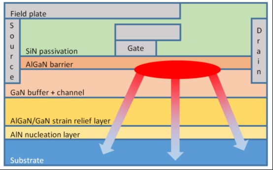
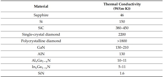
The cross-section view of a general GaN HEMT structure is shown in Figure 1 and the K of the materials typically used are listed in Table 2.The actual structure, composition,and thickness of each layer in a particular HEMT depend on its specific purpose and / or the vendor's manufacturing practices. Since the review and discussion of the literature presenting different devices modifications is out of the scope of this work, only the layers considered relevant to the thermal transport are represented in Figure 1.Other possiblelayers (not shown) would include the spacer and cap layers.

Figure 1. Simplified representation of an AlGaN/GaN HEMT structure; drawing not to scale.
1. Substrate. Homoepitaxial growth of GaN-based films is hampered by the limited availability of GaN substrates in standard wafer sizes. As a consequence, the differentlayers are typically deposited by either Molecular Beam Epitaxy(MBE) or MOCVD onto sapphire, Si, or silicon carbide (SiC) substrates. Epitaxial films with dislocation densities of 108cm-2 are typically obtained; dislocation densities lower than107 cm—2 involve hydride vapor phase epitaxy (HVPE) growth.
2. Nucleation layer. The deposition of high quality epitaxial GaN films with smooth surfaces and low dislocation density is not a straightforward task due to latticemismatch and to the difference in the coefficients of thermal expansion(CTEs) ofGaN and substrate. A nucleation layer, typically 40-200 nm of aluminum nitride(AIN),is thus initially deposited on the substrate surface for strain accommodation and increased interface resistivity.
3. Strain relief layer. AlGaN/GaN transition layers, often up to 1 um thickness, fur-ther accommodate the lattice mismatch during the growth of GaN on the foreign substrate .
4. GaN layer. A 0.6-1.5 um-thick GaN buffer layer that provides electrical isolation toreduce substrate leakage and prevents the propagation of threading dislocations and contaminants that might migrate from the substrate into the top high quality channel region follows.
5. Barrier layer. The typically 5-25 nm-thick barrier layer can be made of AIN,indium gallium nitride (InGaN), or other high bandgap alloys, but AlxGa-xN with an aluminum (Al) fractional content in the range of 22-32% is the most widely reported material.
6. Passivation layer. A thin dielectric layer, typically silicon nitride(Si3N4), compensates the surface/interface states responsible for the current collapse issue by introducing shallow donors.
7. Field plate. The source and gate-connected field plates are usually employed to reduce the strength of the electric field near the gate terminal, reducing the gate tunneling injection current responsible for charging the surface traps.

Table 1.Typical thermal conductivity of the materials present in an AlGaN/GaNHEMT
Most of the heat generated during device operation will diffuse from the hotspot through the different layers represented in Figure 1 until it reaches the heat sink attached to the back of the substrate. A few intrinsic obstacles hinder the transfer of the heat towards the heat sink. The AIGaN/GaN strain relief transition layers improve the electrical performance at the top of the GaN layer, however, if the concentration of Al is higher than 5%, the k of the AlGaN decreases to around 1/10th that of bulk GaN, hampering the transfer of heat from the GaN buffer layer to the underlying substrate .Despite its low thickness in comparison to the GaN layer, the nucleation layer pro-foundly impacts the transport of heat from the strain relief layer towards the underlying substrate. Instead of being composed of high quality AlN, this layer contains dislocations, grain boundaries, and point defects (impurity atoms and vacancies), within the itself or near the interfaces, that hinder heat transport by increasing phonon scattering rates and reducing the phonon mean free path.The interfacial and nucleation layer thermal resistances contribute with an effective TBR between the strain relief layers and the substrate between 10 and 70 m2.K/GW that may cause an additional 30-50% channel temperature rise in AlGaN/GaN HEMTs.
In the search of good thermal conductors, carbon-based materials, such as highly oriented pyrolytic graphite (HOPG), graphene and diamond are obvious candidates. Diamond is an isotropic material with high K(2200 W/(m·K), increasing to 3300 W/(m·K) in the case of isotopically pure material) while being electrically insulating, with a break-down field 60 times greater that of Si (2 x 10⁷V/cm)—Table 2.Single-crystal diamond(SCD), grown by high pressure high temperature (HPHT) method, has the best thermal andelectric properties; however its area is limited to a few mm2. Alternatively, poly crystalline diamond (PCD) films can be grown by chemical vapor deposition(CVD) on large-area substrates such as Si, overcoming the area limitation while still guaranteeing K values in the range 1000-1800 W/(m-K).

Table 2.Selected properties of relevant semiconductors
The GaN-on-diamond concept was initially introduced in 2003. The original idearelied on the deposition of the PCD film directly on the back of the GaN layer. The first GaN-on-diamond wafer pieces were produced in 2004 by etching the Si substrate of a GaN wafer initially deposited by MOCVD, followed by depositing a 50 nm-thick dielectric layer,and then by growing a 25 um-thick PCD film by hot filament CVD(HFCVD).The PCDwas deposited on the Ga-face, leaving behind an N-face GaN-on-diamond wafer after theetching of the temporary Si carrier. The fabrication process remains fundamentally the same till today and is represented in Figure 2.The required steps involved (i) performing the GaN epitaxy on a Si substrate, (ii) bonding the GaN HEMT epilayers onto a temporary Si carrier, (iii) etching away the original host Si substrate, (iv) depositing a 50 nm-thick layer of SiN onto the exposed rear face of the GaN, and (v) depositing a 25 um-thick PCDfilm by HFCVD onto the dielectric. Finally, by (vi) removing the temporary Si carrier, afree-standing GaN-on-diamond wafer was obtained.

Figure 2.GaN-on-diamond fabrication steps.
By 2006, the process had been optimized to fabricate a Ga-face (i.e., right side up)GaN-on-Diamond HEMT epitaxial wafer and the operation of an AlGaN/GaN HEMT with a 25 um-thick PCD film located 1.2 um below the electron channel was reported. The scanning electron microscope(SEM) cross-section of the GaN-on-diamond wafer is shown in Figure 3a. These first unpassivated HEMTs had a high contact resistance that translated in low current capability (maximum drain current ID max = 306 mA/mm) and low peak transconductance(8m peak =70 mS/mm). Further iterations improved the performance ofthe HEMTs , nevertheless, and in spite of having half the thermal resistance Rt:h of GaN-on-SiC HEMTs (≈6 against ≈12K-mm/W, respectively), in 2007 GaN-on-diamond HEMTs were still outperformed by GaN-on-SiC technology—Figure 3b. By 2009 GaN HEMTs with 75 um of PCD showed cut-off (fT) and maximum oscillation (f max) frequenciesof 85 and 95 GHz, respectively , and soon after that the first RF power amplifier module was reported.

Figure 3.(a)SEM cross-section of a GaN-on-diamond wafer (b) Electrical characteristics of similar GaN-on-diamond (solid symbols) and GaN-on-SiC(open symbols)HEMTs;output power and PAE measured at 10 GHz CW class B operation and 20 v VD
The technical indicators of diamond hot sink sheet and diamond wafer products produced by CSMH have reached the world's leading level, the surface roughness of wafer-level diamond growth surface Ra<1nm, and the thermal conductivity of diamond hot deposition sheet has reached 1000-2000W/m.K. By bonding with GaN, the temperature of the device can also be effectively reduced, and the stability and life of the device can be improved. In addition, there are core products such as diamond-based gallium nitride epitaxial sheets, diamond-based aluminum nitride films, etc. At present, diamond heat dissipation products and solutions have been applied in 5G base stations, lasers, high-speed rail, photovoltaics, new energy vehicles and other fields. As a pioneer in the semiconductor industry, we offer you the most comprehensive range of diamond thermal management services.
 闽ICP备2021005558号-1
Leave A Message