Diamond belongs to a new generation of ultra-wide bandgap semiconductor materials, which has a series of advantages such as large band gap, high carrier mobility, high thermal conductivity and good chemical stability, and has important applications in the fields of high frequency, high temperature and high power electronic devices. After the hydrogen terminal diamond formed after the diamond is treated in a hydrogen plasma atmosphere is exposed to the air atmosphere, a layer of two-dimensional hole gas can be formed near the surface of the hydrogen terminal diamond, and the concentration of holes is usually 1012~1014cm-2, and the hole mobility is usually 10~300cm2/Vs. Recently, Liu Jinlong et al. formed a dense thin carbon layer when preparing hydrogen terminals on the surface of high-quality diamonds, achieving hole mobility of up to 365cm2/V·s. Two-dimensional cavitation gas on the surface of hydrogen terminal diamond is widely used in the research of diamond electronic devices.
Field-effect transistors fabricated based on hydrogen terminal diamonds have achieved a cutoff frequency of up to 70GHz, a maximum oscillation frequency of 120GHz, a breakdown voltage of 2kV, and an output power density of 3.8W/mm. Since the formation of two-dimensional cavitation gas on the surface of hydrogen terminal diamond is related to the surface adsorption layer formed by exposure to air, this also leads to the problem of poor conductivity stability on the surface of hydrogen terminal diamond. In order to realize hydrogen terminal diamond field effect transistors, it is found that the use of a medium with a high work function or a medium deposited by ALD as the passivation layer can effectively improve the stability of the device. There have been many reports that ALD-deposed Al2O3 media using H2O as an oxidant are very suitable for the development of hydrogen terminal diamond microwave power field effect transistors. Our previous research has also found that the use of ALD deposition Al2O3 medium at 300°C as the gate dielectric and passivation layer of FET devices can not only effectively improve the stability of the device, but also effectively maintain the carrier concentration on the surface of the hydrogen terminal diamond. After nearly two decades of development, the characteristics of hydrogen terminal diamond field effect transistors have been continuously improved, and have begun to show their huge application potential. Diamond has the advantages of large band gap and high carrier mobility, and has great application potential in future high-temperature logic circuit applications. Therefore, it is also of great significance to study the preparation of diamond logic circuits. Alumina media has been proven to achieve stable high-performance hydrogen terminal diamond MOSFET devices. In this study, an alumina medium deposited at 300°C was used as the gate medium and passivation layer to prepare a hydrogen terminal diamond MOSFET device, and the hydrogen terminal diamond inverter of alumina medium was realized by interconnecting with the resistor prepared on the sheet. The performance of the device and inverter was studied.
In this experiment, single crystal diamond epitaxial by microwave plasma chemical vapor deposition method was used as the substrate. The substrate size is 8mm×8mm×0.5mm, and the substrate is (100) crystal direction. Before proceeding with the preparation process, the substrate is washed in HNO3 and H2SO4 solutions at 250°C for 30 minutes to remove contaminants and non-diamond phase impurities from the substrate surface. Then the substrate was ultrasonically cleaned in acetone, alcohol, and deionized water for 15 minutes. The cleaned single crystal diamond is placed in the microwave plasma chemical vapor deposition system for hydrogen plasma treatment, during the treatment, the hydrogen flow, methane flow, microwave power and pressure are 500sccm, 1sccm, 2kW and 100mbar, the sample surface temperature is 800°C during the treatment, and the processing time lasts 30 minutes. After the treatment is completed, the hydrogen terminal diamond is exposed to the air, forming a two-dimensional cavity gas on the surface of the diamond. After the treatment of the diamond surface, an electron beam evaporation equipment is used to deposit a 100nm thick gold layer, which can effectively protect the two-dimensional cavitation gas on the surface of the hydrogen terminal diamond on the one hand, and the ohmic contact metal as the source leakage electrode on the other hand. Then the contact lithography machine is used for the lithography process, and then the aqueous solution of KI/I2 is used to corrode to form the active region of the device. The sample is then surface treated with low-power oxygen plasma to form device isolation. The gate window is then exposed after the gate window lithography process and the wet corrosion of the gold in the window. Then, using ALD equipment, using H2O as the oxidant, alumina medium was deposited on the surface of the sample at 300 °C with a medium thickness of 15 nm. Then, proceed to the next step of lithography to define the gate of the device. Next, an electron beam evaporation device is used to deposit a layer of aluminum with a thickness of 100 nm as the gate metal. Finally, the preparation of the device is completed by a metal stripping process. During device preparation, the second step of lithography after device isolation is completed simultaneously prepares a resistance pattern on the substrate surface. And by preparing electrodes with different spacing, the resistance preparation of different resistance sizes is realized. The hydrogen terminal diamond MOSFET prepared in this study has a gate length of 4μm, a gate-drain spacing and gate-source spacing of 2μm, and a device gate width of 50μm. Three resistors with different resistance values with electrode spacing of 20μm, 80μm and 160μm were prepared, one end of the resistor was connected to the drainage electrode of the device, and the other end was connected to the DC voltage during the test. The device profile and top-down schematic prepared in this study are shown in Figure 1. Keithley 4200 equipment is used to test device and inverter performance. All tests are performed in room temperature air environment.

Fig. 1 Schematic diagram of (a) section and (b) top view of the experimental prepared device
In order to obtain the resistance values of the three different spacing resistors prepared by the experiment, the current-voltage characteristics of the three resistors prepared by the experiment were first tested. The test results are shown in Figure 2. As can be seen from Figure 2, all three resistors exhibit very good ohmic contact characteristics (Figure 2(a)). It indicates that a good ohmic contact is formed between the gold and the hydrogen terminal diamond. The three resistance values are calculated to be 16.7kΩ, 69.5kΩ and 136.4kΩ, and the resistance value changes linearly with the change of electrode spacing (Fig. 2(b)), which also indicates that the hydrogen terminal diamond prepared by the experiment has good stability.
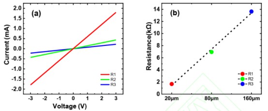
Figure 2 Device load resistance (a) I-V characteristics and (b) resistance value
The output characteristic curve of the device is shown in Figure 3. The 4μm gate length device achieves a maximum output saturation leakage current of 113.4mA/mm at a gate voltage of -6V. This article summarizes the maximum output saturation current density of hydrogen terminal diamond MOSFET devices with different conditions of deposition of alumina dielectric reported in the current literature, as shown in Table 1. It can be seen that the hydrogen terminal diamond MOSFET device prepared in this study using alumina medium grown at 300°C has the maximum output current density reported in alumina dielectric devices with gate length of more than 4μm. From the output curve of the device, it can be calculated that the on-resistance of the device at the -6V gate voltage is 83.68Ω·mm. This on-resistance is equivalent to that of previously reported MOSFET devices.
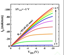
Figure 3 Device output characteristics
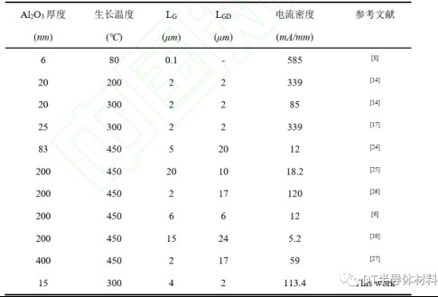
Table 1 Comparison of maximum output current density of hydrogen terminal diamond MOSEFET during deposition of alumina medium under different conditions
Figure 4 shows the saturation region transfer characteristics of the device at a leakage voltage of -10V. From the relationship between gate voltage and square root of leakage current in Figure 4(a) figure, it can be obtained that the threshold voltage of the device is 5.2V, and the 7-terminal diamond MOSFET prepared by the experiment is a depletion device. The device achieves maximum transconductance of up to 24mS/mm at -0.2V gates. From the transfer curve of the logarithmic coordinates of the device in Figure 4(b), the switching ratio of the device reaches more than 109, and the gate leakage current determines the off-state leakage of the device. The minimum subthreshold swing of the device is 117mV/dec.
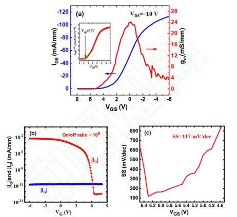
Figure 4 Device transfer characteristics
Finally, we test the inverter DC voltage transfer characteristics under various load resistors prepared experimentally, and the results are shown in Figure 5. The circuit schematic of the inverter is given in the illustration. During the test, VDD applied a constant voltage of 10V. As Vin changes from 12V to 0V, we observe inverter characteristics for all load resistance cases. When || At <||, the="" diamond="" mosfet="" device="" shuts="" and="" current="" from="" vdd="" to="" ground="" is="" almost="" so="" output="" voltage="" vout="" 0v.="">|| , the diamond MOSFET device is turned on, the output voltage Vout is the voltage divider between the on-resistance and the load resistance, and the on-resistance of the device is much smaller than the load resistance value, so the output voltage Vout is 10V. It can be seen that when the input is high, the output is low, and when the input is low, the output is high, that is, the inverter characteristics are realized. It can also be seen from Figure 5 that as the load resistance increases, the output is lower low.
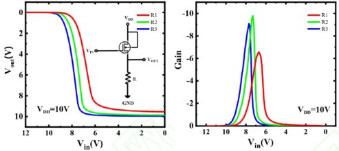
Figure 5 Reverse characteristics of different load resistors Figure 6 Input voltage vs. load plot
The gain vs. input voltage for different load resistances of this inverter is calculated as shown in Figure 6. As the load resistance increases, the Vin value of the maximum value of the inverter gain shifts to the left, and as the load resistance value increases, the inverter gain shows a trend of first increasing and then decreasing, and the maximum gain is 10.The inverter gain is defined as the ratio of the output voltage change rate to the input voltage change rate (dVout/dVin), and the circuit satisfies: VDD=VDS+Vout=VDS+IDRD, and the load line is shown in the figure on the output characteristic curve. As the RD increases, the intersection point of the load line and the ordinate ID shifts down. As shown in Figure 7(a), when the device operates in the constant current region, the rate of change of the output voltage Vout gradually increases as the RD increases, and the output voltage Vout gradually increases, so the inverter gain increases. As shown in Figure 7(b), when the device operates in the variable resistance region, the rate of change of the output voltage Vout gradually decreases as the RD increases, and the fixed input voltage, so the inverter gain decreases. At the maximum load resistance, when Vin = 8V, RD=136.4kΩ, Vout = 7.6V, the calculation can be obtained: | VDS|=2.4V,| VGS|-| VTH|=3.1V, so the device has entered the variable resistor region and the gain is reduced.
In this study, the characteristics of diamond inverters were successfully prepared and tested, indicating that ultra-wide bandgap semiconductor diamonds have the potential for application in digital circuits. In the future, the performance of diamond inverters will be further improved by improving the device characteristics, and the static power consumption of the inverter will be reduced by preparing diamond-enhanced devices.
CSMH adopts the most advanced MPCVD device to prepare large-area high-quality diamond hot sink with thermal conductivity of 1000-2000W/m.k, high thickness uniformity and high growth rate; the surface roughness of diamond wafer growth surface Ra < 1 nm using special equipment for grinding and polishing. At present, diamond hot dissipation products and solutions have been applied in 5G base stations, lasers, high-speed rail, new energy vehicles, national defense industry and other fields, and we will continue to develop and innovate products and innovations in the future, and contribute new strength to scientific and technological progress!
 闽ICP备2021005558号-1
Leave A Message