Pos:
Home KnowledgeTechnologyThe application frontier of diamond - diamond wafer resistance made of a single piece on a diamond fIt is well known that one of the electronic properties of diamond is its dual use as a medium or semiconductor. Undoped diamond suppresses resistivity up to 10 to the 14th power ~ 10 to the 16th power Ω-cm, but can be made highly conductive (<1Ω-cm) by boron doping. The conductivity control ability of doped semiconductors is an indispensable condition for the preparation of millisecond-level electronic devices. This doping control has been controlled in single crystals and also has an effect on the polycrystalline properties of p-type boron doping. Another criterion for achieving actual diamond electronics is the ability to separate conductive diamonds from non-conductive areas. The ability of diamonds to make molds, as well as the ability to apply certain microelectronic processes to polydiamond terephthalate films, was studied, and the problem of electrical isolation was studied. Although it is related both to the resistance characteristics of diamonds and to their practical value in practical electronic devices (resistors, capacitors and transistors). Conductive diamonds are prepared on dielectric substrates (aluminum nitride, quartz), but these structures do not use diamond as an insulator and semiconductor material. If the substrate is not insulating and leakage is allowed, the electrical properties of the doped patterned diamond region cannot be applied to the actual device. In order to form a useful all-diamond electronic device structure, a patterned doped diamond film must be grown on a single crystal substrate.
The process flow to realize the diamond structure is shown in Figure 1. The sub-beam is a single epitaxial β-SiC layer, generally 10 μm thick, thickness (I00) Si Before growth, the SiC surface is polished with a coarse particle size of 0.1 μm. The result of this method is an increase in the nucleation density of the crystal, which allows it to form a uniform, continuous layer. Massive deposits on the SiC surface result in sporadic patches.
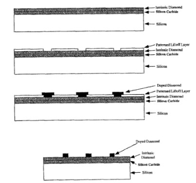
Figure 1 Diamond-SiC substrate manufacturing process specification for diamond resistors
Deposition of undoped diamond layers. To form an isolated diamond resistance network on a SiC substrate, an intrinsic diamond layer is grown, followed by a patterned doping layer. Under the diamond deposition conditions of Si, a continuous, pinhole-free polydiamond layer, approximately 10 μm thick, grows on the SiC substrate within 20 hours. The Raman spectrum of the thin film (see Figure 2) indicates that the deposited layer is polydiamond. When these layers are probed, no conductivity is observed.
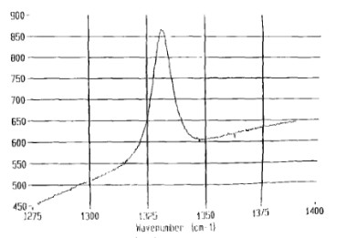
Figure 2 Raman spectra of polycrystalline diamonds grown on SiC substrates (note the extended wavelength scale).
Pattern and resistance formation of diamond films. To achieve a patterned resistive structure, a selective deposition/peeling process was developed. Sputtering SiO2 is used as a sacrificial peeling layer. Under the deposition conditions used in these processes, diamonds tend to occasionally nucleate on SiO2. After diamond deposition, the exposed SiO2 is removed by H20:HF (10:1) etching. SiO2 is deposited on a layer of i-diamond (undoped inner surface) and patterned by photolithography. Subsequently, a layer of doped diamond was deposited. The nucleation process associated with doped diamond formation occurs almost exclusively on exposed type I diamonds and not on the SiO2 layer. SiO2 is then etched with HF to remove SiO2. The pattern transfer from silica is effective, resulting in well-defined features on doped diamonds.
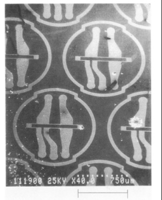
Figure 3 SEM image at low magnification, labeled 750μm, showing multiple diamond resistive elements. The shallower area is the doped diamond resistance
The p-type diamond resistance structure in Figure 3 is detected at room temperature with a tungsten probe. A typical example is a 1cm2 sample containing more than 120 complete test resistors. There is a pattern SiO2 of 1 μm on type I diamond, and the doped medium deposition time is 1 h. SiO2 was removed in HF etching and then etched in H2 plasma for 30 min. The final structure consists of 4 layers: silicon (400 μm); Epitaxial SiC (8 ~ 10μm);
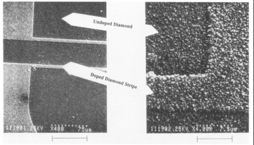
Figure 4 (Left) High-magnification SEM image, labeled 75 μm, showing doped and unadulterated regions. (Right) Magnification of 7.5μm.
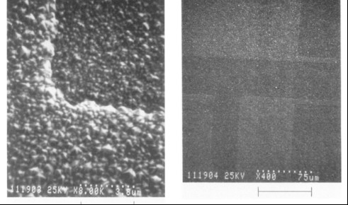
Figure 5 When zoomed in, the mark point is 3.8 μm (left).
Fig. 6 SEM image of diamond surface with eroded SiO2 peel layer and diamond doping on the entire surface, marking point 75μm (right figure).
Probe measurements are performed on resistance between isolated p-diamond regions, as well as on i-diamond (see Figure 8). The following results were obtained at many sites on the specimen for different devices: (i) RAB ~ ~ 7 to 20 Ω, and (ii) RAc = RAo = open. (Rij is the resistance measured between points A, B, C, and D in Figure 8.) No current flow is detected between adjacent patterns and between resistors and substrates. The detection limit is less than 1pa. Therefore, the isolation ratio (current/leakage) is greater than 10%. Figure 9 is an I-V plot of a representative resistor pattern. According to the resistance value and resistance size, the resistivity of the film is determined in the range of 10 ~ 20Ω/cm.
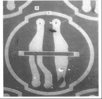
Figure 7 Resistor pattern identification probe contact point for electrical measurement
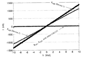
Figure 8 Current-voltage behavior of p-diamond resistors on diamond/SiC substrates
CSMH is a high-tech enterprise focusing on the research and development and production of third-generation (wide bandgaping) semiconductor substrate materials and devices, and is committed to becoming the world's leading wide bandgap semiconductor materials and device company. We have always adhered to the concept of customer first, to provide customers with the best products and services. At present, the company has realized the large-scale production of diamond and aluminum nitride related products. Existing diamond wafer Ra<1nm, diamond hot sink thermal conductivity 1000-2000W/m.k, and GaN on diamond, Diamond on GaN, diamond-based aluminum nitride and other products. And the products have been widely used in 5G base stations, lasers, new energy vehicles, new energy photovoltaics, aerospace and national defense and other fields.
 闽ICP备2021005558号-1
Leave A Message