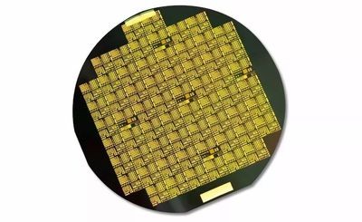
Diamond Wafer Enables More Prolific Chips as Global Industry Races to Manufacturer Smaller, More Powerful Semiconductors and Extend Moore’s Law.
AKHAN Semiconductor (AKHAN), a technology company specializing in the fabrication and application of synthetic, lab-grown electronics-grade diamond materials addressing semiconductor, telecom, and consumer industries and global markets, today showcased the ability to manufacture 300MM complementary metal–oxide–semiconductor (CMOS) diamond wafers. An industry breakthrough, 300MM CMOS diamond wafers will enhance power handling, heat management and durability of electronics across industries with little change to fabricators’ existing manufacturing processes.
Due to its inherent properties, diamond is proven to be the most optimal semiconductor material, far outmatching the capabilities of silicon, the industry-standard material for more than six decades. To produce the world’s most advanced technologies, semiconductor fabricators traditionally rely on 300MM silicon wafers despite the fact that silicon has reached its physical limitations. As the global industry advances beyond Moore’s Law, the ability to produce 300MM diamond wafers is crucial to semiconductor fabricators, especially in advanced industries like aerospace, telecommunications, military and defense, and consumer electronics.
The semiconductor chip shortage has been well documented this year,As the U.S. plans to increase chip supply, it is also important to fabricate using the best materials available to enable the best performance.
AKHAN’s 300MM diamond wafer is the foundational building block that will lead to more powerful and durable devices that run cooler, and fabricators only need to make minor updates to their existing manufacturing processes,From weapon systems to spacecraft, the world’s most sophisticated devices and technologies stand to benefit exponentially from diamond. Now that we’ve proven the ability to manufacture this ideal material on 300MM wafers, fabricators will have access to the most optimal chip material so that their end products perform far more efficiently.
We are committed to the research and development and production of diamonds. Now we have diamond heat sinks, wafer-level diamonds and other products, which have a wide range of applications in military and other fields.

 闽ICP备2021005558号-1
Leave A Message