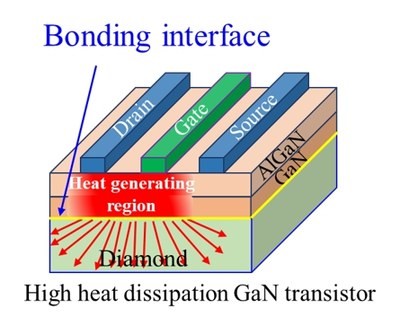
“Researchers have successfully bonded diamond to GaN directly at room temperature, demonstrating that the bond can withstand heat treatment at 1,000 ° C, making it ideal for high-temperature manufacturing processes for GaN-based devices.” Osaka City University says. , The home of the project.
Not surprisingly, attempts have already been made to create GaN on diamond using some form of transition or adhesive layer, but additional layers interfere with thermal conductivity and “crystal structure and lattice constants”. The big difference is that diamonds grow directly. With GaN, the reverse is not possible, “said OCU engineer Jianbo Liang.
Direct wafer bonding at high temperatures (usually 500 ° C) was possible, but the thermal mismatch caused cracks in the bonding results.
Osaka CUGaN photo 345 on diamondThe answer was “surfactant binding” (SAB). The surfaces are atomically cleaned and activated so that they react when they come into contact with each other.
“The chemistry of GaN is completely different from the materials the research team used in the past, so after using SAB to create a GaN material on diamond, a variety of techniques are used to stabilize the bond site. I tested it, “said OCU.
They used Raman spectroscopy, transmission electron microscopy, and energy dispersive X-ray spectroscopy to evaluate the structure and atomic behavior of GaN diamonds. Electron energy loss spectroscopy reveals how carbon atoms are bonded and then provides joint stability in nitrogen at 700 ° C, which is required when manufacturing GaN power devices. I tested it.
Osaka CUGaN on diamond micrograph 297The results showed that a layer of mixed amorphous carbon and diamond about 5 nm thick was formed, infiltrated with diffused gallium and nitrogen atoms. There was some residual compressive stress, but less than what remained after GaN crystal growth on diamond.
Increasing the annealing temperature turns the amorphous carbon into diamond, which thins the layer.
After annealing at 1,000 ° C, the layer is reduced to 1.5 nm, “suggesting that the intermediate layer can be completely removed by optimizing the annealing process,” said engineer Professor Naoki Shigekawa.
“No delamination was observed at the hetero interface after annealing at 1000 ° C, so these results indicate that the GaN-diamond interface can withstand the rigors of the manufacturing process,” says Liang.
Work on Advanced MaterialsManufacture of GaN / diamond hetero-interfaces and surface chemical bonds for highly efficient device design.
 闽ICP备2021005558号-1
Leave A Message