With the large-scale application of the third generation of semiconductors and the advent of the 5G era, traditional electronic packaging thermal management materials and even chip materials are facing great challenges in upgrading, and the rapid rise of advanced carbon and its composite materials in recent years will play an important role in the field of heat dissipation of high-power, high-frequency optoelectronic devices, and become an ideal thermal management material in the electronics industry! (including heat sink materials, packaging materials, matrix materials, substrate materials, etc.). Electronic packaging materials are used to carry electronic components and their interconnections, mainly playing the role of mechanical support, sealing protection, heat dissipation and shielding, etc., which have a very important impact on the performance and reliability of integrated circuits. With the development of electronic technology, integrated circuits are developing in the direction of ultra-large-scale, ultra-high-speed, high-density, high-power, high-precision and multi-function, so that higher and higher requirements are put forward for packaging, substrate and heat sink and other materials.

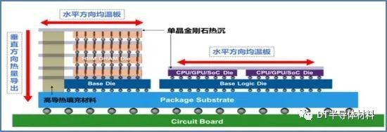
Figure1.Diamond packaging technology
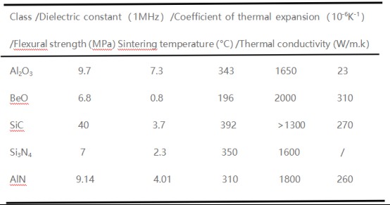
The requirements of packaging materials are: high resistivity, high thermal conductivity, low dielectric constant, dielectric loss, good thermal matching with silicon and gallium arsenide, high surface flatness, good mechanical properties and easy industrial production. General packaging materials are Al2O3 ceramics, SiC ceramics, and AlN materials. However, the thermal expansion coefficient of Al2O3 (7.2×10⁻⁶/°C) and dielectric constant (9.7) are high compared with Si single crystals, and the thermal conductivity (15-35W/ (m·K)) is still not high enough, resulting in Al2O3 ceramic substrates are not suitable for use in high-frequency and high-power electronic devices. The thermal conductivity of SiC ceramics is very high, and the higher the purity of SiC crystallization, the greater the thermal conductivity. The biggest disadvantage of SiC is that the dielectric constant is too high, and the dielectric strength is low, which limits its high-frequency application and is only suitable for low-density packaging and packaging; AlN material has excellent dielectric properties and stable chemical properties, especially its thermal expansion coefficient is more compatible with silicon and other characteristics make it a promising semiconductor packaging material, but the thermal conductivity can only be 260W/ (m·K), with the higher and higher requirements of electronic device packaging, AlN materials also have certain development bottlenecks. Diamond is currently known to have the highest thermal conductivity in nature, the thermal conductivity of diamond thermal sink sheet can be as high as 2000 W/(m.K), thermal expansion coefficient of about 1.1×10⁻⁶/°C, is the most competitive packaging material.

Figure 2 Comparison of diamond with other encapsulation materials
2. Diamond substrate technology
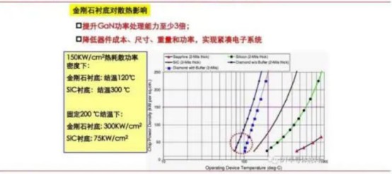
With the increase of output power of gallium nitride (GaN)-based microwave power devices and the reduction of device size, heat dissipation has become one of the important factors restricting their reliability and stability. Heat generation during transistor operation and degradation and reliability degradation due to temperature rise have always been serious problems for transistors of all types and materials. In particular, GaN transistors must develop effective heat dissipation methods due to their higher output power and frequency compared to current mainstream silicon transistors.

Figure 3 Diamond substrate to increase gallium nitride power processing, cost reduction, size and weight description
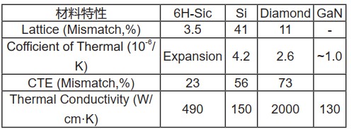
Among the natural substances currently known, diamond has the highest thermal conductivity and is an indispensable heat dissipation material for the preparation of GaN-based electronic devices, and has great application potential in the heat dissipation of high-frequency high-power AlGaN/GaN high-electron mobility transistors.

Figure 4 Properties of several common substrate materials
As a high-tech enterprise focusing on the R&D and production of third-generation (wide bandgap) semiconductor substrate materials and devices, CSMH is committed to becoming the world's leading wide bandgap semiconductor materials and device companies. Currently, we offer three combinations of diamond and GaN: GaN on diamond, Diamond on GaN and diamond wafer (Ra<1nm) required for diamond-to-GaN bonding, Ra<0.5nm for customized products), and diamond heat sink thermal conductivity up to 1000-2000W/m.k. To provide you with the most complete diamond thermal management solutions, in the future, we will continue to improve product quality through manufacturing intelligence, optimization of production technology and other measures, in line with the international advanced management level.
 闽ICP备2021005558号-1
Leave A Message