The development of third-generation semiconductors such as GaN and SiC has driven power devices towards higher power, miniaturization, integration, and multifunctionality. With the improvement of integration and the reduction of volume, the power consumption per unit volume continues to increase, leading to an increase in heat and a sharp rise in temperature. Therefore, heat dissipation has become a bottleneck problem hindering the development of high-power electronic devices.
In terms of heat dissipation substrates for high-power components and systems, matching thermal management materials with thermal conductivity, thermal expansion coefficients that match semiconductor chip materials (Si or GaAs), sufficient stiffness and strength, and lower costs are required.
Diamond is one of the materials with the highest thermal conductivity in nature, with a thermal conductivity between 1000 and 2200 W/(m.K), which is tens or even hundreds of times higher than other ceramic substrate materials. It has excellent thermal, optical, and semiconductor properties, and its coefficient of expansion is relatively low, about 1.1 × 10⁻⁶/℃. As a packaging material, diamond exhibits excellent performance.

As early as the 1960s, attempts were made to use diamond as a heat dissipation material. Diamond is a material with extremely high thermal conductivity and hardness, often used for heat dissipation in high-power density and high-frequency electronic devices. Diamond is mainly used as a heat sink material in two forms, namely diamond film and composite of diamond with metals such as copper and aluminum.
Both diamond and copper have high thermal conductivity (copper has a thermal conductivity of 397W/(m · K)), and their lattice constants are similar. However, the two also have some problems, such as significant differences in thermal expansion coefficients and poor adhesion (copper and carbon do not wet each other, and copper does not melt in diamond). During the production process, the issue of adhesion was solved by utilizing intermediate layers such as Ti Pt Au, Ti, Mo, and Ta.
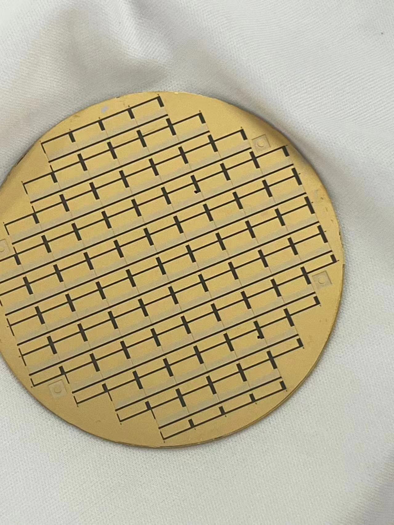
The process flow for producing diamond packaging substrates is as follows: first, clean the surface of the diamond and then dry it. Then, use magnetron sputtering to coat the surface with a layer of titanium metal, and then coat it with a layer of copper metal to ensure the adhesion between the diamond substrate and the metal. Then, the circuit pattern is formed through steps such as circuit exposure, development, electroplating, etching, etc. In this process, it is also necessary to overcome the negative impact of high diamond hardness during the machining process to ensure the performance of the diamond packaging substrate is guaranteed.

CSMH is committed to the production and research and development of diamond materials, mastering mature heat dissipation solutions for high-power devices, and providing services such as metalization, graphitization, and drilling. Its core products include diamond wafer, diamond heat sink, diamond window, and diamond heterojunction integrated composite substrates. Among them, the surface roughness the diamond wafer Ra is less than 1 nm, and the thermal conductivity of the diamond heat sink is 1000-2000W/(m.K), which has been applied in high-power lasers, LEDs, new energy vehicle IGBTs, medical devices and other fields.
 闽ICP备2021005558号-1
Leave A Message